TMP86FH46ANG(Z) Toshiba, TMP86FH46ANG(Z) Datasheet - Page 76
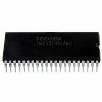
TMP86FH46ANG(Z)
Manufacturer Part Number
TMP86FH46ANG(Z)
Description
IC MCU 8BIT FLASH 16KB 42-SDIP
Manufacturer
Toshiba
Series
TLCS-870/Cr
Datasheet
1.TMP86FH46ANGZ.pdf
(214 pages)
Specifications of TMP86FH46ANG(Z)
Core Processor
870/C
Core Size
8-Bit
Speed
16MHz
Connectivity
SIO, UART/USART
Peripherals
LED, PWM, WDT
Number Of I /o
33
Program Memory Size
16KB (16K x 8)
Program Memory Type
FLASH
Ram Size
512 x 8
Voltage - Supply (vcc/vdd)
2.7 V ~ 5.5 V
Data Converters
A/D 8x10b
Oscillator Type
Internal
Operating Temperature
-40°C ~ 85°C
Package / Case
42-SDIP (0.600", 15.24mm)
Processor Series
TLCS-870
Core
870/C
Data Bus Width
8 bit
Data Ram Size
512 B
Interface Type
SIO, UART
Maximum Clock Frequency
16 MHz
Number Of Programmable I/os
33
Number Of Timers
3
Maximum Operating Temperature
+ 85 C
Mounting Style
Through Hole
Development Tools By Supplier
BMSKTOPAS86FH47(AND), BM1040R0A, BMP86A100010A, BMP86A100010B, BMP86A200010B, BMP86A200020A, BMP86A300010A, BMP86A300020A, BMP86A300030A, SW89CN0-ZCC, SW00MN0-ZCC
Minimum Operating Temperature
- 40 C
On-chip Adc
10 bit, 8 Channel
For Use With
BM1401W0A-G - FLASH WRITER ON-BOARD PROGRAMTMP86C909XB - EMULATION CHIP FOR TMP86F SDIP
Lead Free Status / RoHS Status
Lead free / RoHS Compliant
Eeprom Size
-
Lead Free Status / Rohs Status
Details
Other names
TMP86FH46ANGZ


7.1 Port P0 (P07 to P00)
7.1 Port P0 (P07 to P00)
P0PRD
(0008H)
Read only
(0000H)
input, serial interface input/output and timer/counter input/output.
When used as an output port, the respective P0DR bit should be set to “0”. During reset, the output latch is initial-
ized to “1”.
ister should be read.
EINTCR). During reset, P00 port (
P0DR
R/W
Port P0 is an 8-bit input/output port which is also used as an external interrupt input, Serial PROM mode control
P0 port output latch (P0DR) and P0 port terminal input (P0PRD) are located on their respective address.
When read the output latch data, the P0DR should be read and when read the terminal input data, the P0PRD reg-
P00 port (
When used as an input port or a secondary function pins, the respective output latch (P0DR) should be set to “1”.
Output latch data (P0DR)
INT4
P07
P07
7
7
INT0
Port data (P0PRD)
) can be configured as either an I/O port or as external interrupt input with INT0EN (bit in
Control output
P06
SCK
P06
Control input
6
6
Data output
OUTEN
STOP
P05
P05
SI
5
5
INT0
P04
P04
SO
4
4
Output latch
) is configured as an input port.
D
Figure 7-2 Port 0
Q
TXD
P03
P03
3
3
Page 62
BOOT
RXD
P02
P02
2
2
PWM4
PDO4
PPG4
P01
TC4
P01
1
1
P00
INT0
P00
0
0
(Initial value: 1111 1111)
P0i
Note: i = 7
to
TMP86FH46ANG
0
Related parts for TMP86FH46ANG(Z)
Image
Part Number
Description
Manufacturer
Datasheet
Request
R

Part Number:
Description:
Toshiba Semiconductor [TOSHIBA IGBT Module Silicon N Channel IGBT]
Manufacturer:
TOSHIBA Semiconductor CORPORATION
Datasheet:
Part Number:
Description:
TOSHIBA GTR MODULE SILICON NPN TRIPLE DIFFUSED TYPE
Manufacturer:
TOSHIBA Semiconductor CORPORATION
Datasheet:
Part Number:
Description:
TOSHIBA GTR Module Silicon N Channel IGBT
Manufacturer:
TOSHIBA Semiconductor CORPORATION
Datasheet:
Part Number:
Description:
TOSHIBA Intelligent Power Module Silicon N Channel IGBT
Manufacturer:
TOSHIBA Semiconductor CORPORATION
Datasheet:
Part Number:
Description:
TOSHIBA INTELLIGENT POWER MODULE SILICON N CHANNEL LGBT
Manufacturer:
TOSHIBA Semiconductor CORPORATION
Datasheet:
Part Number:
Description:
TOSHIBA IGBT Module Silicon N Channel IGBT
Manufacturer:
TOSHIBA Semiconductor CORPORATION
Datasheet:
Part Number:
Description:
TOSHIBA GTR MODULE SILICON N−CHANNEL IGBT
Manufacturer:
TOSHIBA Semiconductor CORPORATION
Datasheet:
Part Number:
Description:
TOSHIBA Intelligent Power Module Silicon N Channel IGBT
Manufacturer:
TOSHIBA Semiconductor CORPORATION
Datasheet:
Part Number:
Description:
TOSHIBA GTR Module Silicon N Channel IGBT
Manufacturer:
TOSHIBA Semiconductor CORPORATION
Datasheet:
Part Number:
Description:
TOSHIBA INTELLIGENT POWER MODULE
Manufacturer:
TOSHIBA Semiconductor CORPORATION
Datasheet:
Part Number:
Description:
TOSHIBA Intelligent Power Module Silicon N Channel IGBT
Manufacturer:
TOSHIBA Semiconductor CORPORATION
Datasheet:
Part Number:
Description:
TOSHIBA Intelligent Power Module Silicon N Channel IGBT
Manufacturer:
TOSHIBA Semiconductor CORPORATION
Datasheet:
Part Number:
Description:
TOSHIBA IGBT Module Silicon N Channel IGBT
Manufacturer:
TOSHIBA Semiconductor CORPORATION
Datasheet:
Part Number:
Description:
TOSHIBA Intelligent Power Module Silicon N Channel IGBT
Manufacturer:
TOSHIBA Semiconductor CORPORATION
Datasheet:
Part Number:
Description:
Toshiba Semiconductor [SILICON N CHANNEL 1GBT]
Manufacturer:
TOSHIBA Semiconductor CORPORATION
Datasheet: