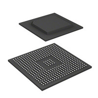
R8A77850ANBGV Renesas Electronics America, R8A77850ANBGV Datasheet - Page 220

R8A77850ANBGV
Manufacturer Part Number
R8A77850ANBGV
Description
IC SUPERH MPU ROMLESS 436-BGA
Manufacturer
Renesas Electronics America
Series
SuperH® SH7780r
Datasheet
1.R8A77850AADBGV.pdf
(1694 pages)
Specifications of R8A77850ANBGV
Core Processor
SH-4A
Core Size
32-Bit
Speed
600MHz
Connectivity
Audio Codec, MMC, Serial Sound, SCI, SIO, SPI, SSI
Peripherals
DMA, POR, WDT
Number Of I /o
108
Program Memory Type
ROMless
Ram Size
8K x 8
Voltage - Supply (vcc/vdd)
1 V ~ 1.2 V
Oscillator Type
External
Operating Temperature
-20°C ~ 75°C
Package / Case
436-BGA
Lead Free Status / RoHS Status
Lead free / RoHS Compliant
Eeprom Size
-
Program Memory Size
-
Data Converters
-
Available stocks
Company
Part Number
Manufacturer
Quantity
Price
Company:
Part Number:
R8A77850ANBGV
Manufacturer:
Renesas Electronics America
Quantity:
10 000
- Current page: 220 of 1694
- Download datasheet (9Mb)
7. Memory Management Unit (MMU)
7.6.7
An initial page write exception occurs when the D bit is 0 even though a UTLB entry contains
address translation information matching the virtual address to which a data access (write) is
made, and the access is permitted. The initial page write exception processing carried out by
hardware and software is shown below.
(1)
In the event of an initial page write exception, hardware carries out the following processing:
1. Sets the VPN of the virtual address at which the exception occurred in PTEH.
2. Sets the virtual address at which the exception occurred in TEA.
3. Sets exception code H'080 in EXPEVT.
4. Sets the PC value indicating the address of the instruction at which the exception occurred in
5. Sets the SR contents at the time of the exception in SSR. The R15 contents at this time are
6. Sets the MD bit in SR to 1, and switches to privileged mode.
7. Sets the BL bit in SR to 1, and masks subsequent exception requests.
8. Sets the RB bit in SR to 1.
9. Branches to the address obtained by adding offset H'0000 0100 to the contents of VBR, and
(2)
Software is responsible for the following processing:
1. Retrieve the necessary page table entry from external memory.
2. Write 1 to the D bit in the external memory page table entry.
3. In TLB compatible mode, write to PTEL the values of the PPN, PR, SZ, C, D, SH, V, and WT
4. When the entry to be replaced in entry replacement is specified by software, write that value to
Rev.1.00 Jan. 10, 2008 Page 188 of 1658
REJ09B0261-0100
SPC. If the exception occurred at a delay slot, sets the PC value indicating the address of the
delayed branch instruction in SPC.
saved in SGR.
starts the initial page write exception handling routine.
bits in the page table entry stored in the address translation table for external memory.
In TLB extended mode, write to PTEL and PTEA the values of the PPN, EPR, ESZ, C, D, SH,
V, and WT bits in the page table entry stored in the address translation table for external
memory.
the URC bits in MMUCR. If URC is greater than URB at this time, the value should be
changed to an appropriate value after issuing an LDTLB instruction.
Hardware Processing
Software Processing (Initial Page Write Exception Handling Routine)
Initial Page Write Exception
Related parts for R8A77850ANBGV
Image
Part Number
Description
Manufacturer
Datasheet
Request
R

Part Number:
Description:
KIT STARTER FOR M16C/29
Manufacturer:
Renesas Electronics America
Datasheet:

Part Number:
Description:
KIT STARTER FOR R8C/2D
Manufacturer:
Renesas Electronics America
Datasheet:

Part Number:
Description:
R0K33062P STARTER KIT
Manufacturer:
Renesas Electronics America
Datasheet:

Part Number:
Description:
KIT STARTER FOR R8C/23 E8A
Manufacturer:
Renesas Electronics America
Datasheet:

Part Number:
Description:
KIT STARTER FOR R8C/25
Manufacturer:
Renesas Electronics America
Datasheet:

Part Number:
Description:
KIT STARTER H8S2456 SHARPE DSPLY
Manufacturer:
Renesas Electronics America
Datasheet:

Part Number:
Description:
KIT STARTER FOR R8C38C
Manufacturer:
Renesas Electronics America
Datasheet:

Part Number:
Description:
KIT STARTER FOR R8C35C
Manufacturer:
Renesas Electronics America
Datasheet:

Part Number:
Description:
KIT STARTER FOR R8CL3AC+LCD APPS
Manufacturer:
Renesas Electronics America
Datasheet:

Part Number:
Description:
KIT STARTER FOR RX610
Manufacturer:
Renesas Electronics America
Datasheet:

Part Number:
Description:
KIT STARTER FOR R32C/118
Manufacturer:
Renesas Electronics America
Datasheet:

Part Number:
Description:
KIT DEV RSK-R8C/26-29
Manufacturer:
Renesas Electronics America
Datasheet:

Part Number:
Description:
KIT STARTER FOR SH7124
Manufacturer:
Renesas Electronics America
Datasheet:

Part Number:
Description:
KIT STARTER FOR H8SX/1622
Manufacturer:
Renesas Electronics America
Datasheet:

Part Number:
Description:
KIT DEV FOR SH7203
Manufacturer:
Renesas Electronics America
Datasheet:


