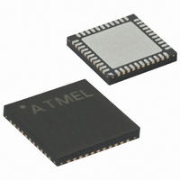
ATMEGA324P-A15MZ Atmel, ATMEGA324P-A15MZ Datasheet - Page 108

ATMEGA324P-A15MZ
Manufacturer Part Number
ATMEGA324P-A15MZ
Description
MCU AVR 32KB FLASH 15MHZ 44-VQFN
Manufacturer
Atmel
Series
AVR® ATmegar
Datasheet
1.ATMEGA324P-A15MZ.pdf
(346 pages)
Specifications of ATMEGA324P-A15MZ
Package / Case
44-VQFN Exposed Pad
Voltage - Supply (vcc/vdd)
2.7 V ~ 5.5 V
Operating Temperature
-40°C ~ 125°C
Speed
16MHz
Number Of I /o
32
Eeprom Size
1K x 8
Core Processor
AVR
Program Memory Type
FLASH
Ram Size
2K x 8
Program Memory Size
32KB (32K x 8)
Data Converters
A/D 8x10b
Oscillator Type
Internal
Peripherals
Brown-out Detect/Reset, POR, PWM, WDT
Connectivity
I²C, SPI, UART/USART
Core Size
8-Bit
Lead Free Status / RoHS Status
Lead free / RoHS Compliant
- Current page: 108 of 346
- Download datasheet (3Mb)
108
ATmega32(L)
Table 45. Compare Output Mode, Fast PWM
Note:
Table 46
rect or the phase and frequency correct, PWM mode.
Table 46. Compare Output Mode, Phase Correct and Phase and Frequency Correct PWM
Note:
• Bit 3 – FOC1A: Force Output Compare for Compare unit A
• Bit 2 – FOC1B: Force Output Compare for Compare unit B
The FOC1A/FOC1B bits are only active when the WGM13:0 bits specifies a non-PWM mode.
However, for ensuring compatibility with future devices, these bits must be set to zero when
TCCR1A is written when operating in a PWM mode. When writing a logical one to the
FOC1A/FOC1B bit, an immediate compare match is forced on the Waveform Generation unit.
The OC1A/OC1B output is changed according to its COM1x1:0 bits setting. Note that the
FOC1A/FOC1B bits are implemented as strobes. Therefore it is the value present in the
COM1x1:0 bits that determine the effect of the forced compare.
COM1A1/COM1B1
COM1A1/COM1B1
1. A special case occurs when OCR1A/OCR1B equals TOP and COM1A1/COM1B1 is set. In
1. A special case occurs when OCR1A/OCR1B equals TOP and COM1A1/COM1B1 is set.
shows the COM1x1:0 bit functionality when the WGM13:0 bits are set to the phase cor-
0
0
1
1
0
0
1
1
this case the compare match is ignored, but the set or clear is done at BOTTOM.
PWM Mode” on page 99.
“Phase Correct PWM Mode” on page 101.
COM1A0/COM1B0
COM1A0/COM1B0
0
1
0
1
0
1
0
1
for more details.
Description
Normal port operation, OC1A/OC1B
disconnected.
WGM13:0 = 15: Toggle OC1A on Compare
Match, OC1B disconnected (normal port
operation).
For all other WGM13:0 settings, normal port
operation, OC1A/OC1B disconnected.
Clear OC1A/OC1B on compare match, set
OC1A/OC1B at BOTTOM,
(non-inverting mode)
Set OC1A/OC1B on compare match, clear
OC1A/OC1B at BOTTOM,
(inverting mode)
Description
Normal port operation, OC1A/OC1B
disconnected.
WGM13:0 = 9 or 14: Toggle OC1A on
Compare Match, OC1B disconnected (normal
port operation).
For all other WGM13:0 settings, normal port
operation, OC1A/OC1B disconnected.
Clear OC1A/OC1B on compare match when
up-counting. Set OC1A/OC1B on compare
match when downcounting.
Set OC1A/OC1B on compare match when up-
counting. Clear OC1A/OC1B on compare
match when downcounting.
(1)
for more details.
2503N–AVR–06/08
See “Fast
(1)
See
Related parts for ATMEGA324P-A15MZ
Image
Part Number
Description
Manufacturer
Datasheet
Request
R

Part Number:
Description:
Manufacturer:
Atmel Corporation
Datasheet:

Part Number:
Description:
Manufacturer:
Atmel Corporation
Datasheet:

Part Number:
Description:
IC MCU AVR 32K FLASH 44-TQFP
Manufacturer:
Atmel
Datasheet:

Part Number:
Description:
IC MCU AVR 32K FLASH 44-QFN
Manufacturer:
Atmel
Datasheet:

Part Number:
Description:
IC MCU AVR 32K FLASH 40-DIP
Manufacturer:
Atmel
Datasheet:

Part Number:
Description:
MCU AVR 32K FLASH 20MHZ 44-QFN
Manufacturer:
Atmel
Datasheet:

Part Number:
Description:
MCU AVR 32KB FLASH 20MHZ 44TQFP
Manufacturer:
Atmel
Datasheet:

Part Number:
Description:
MCU AVR 32KB FLASH 20MHZ 44QFN
Manufacturer:
Atmel
Datasheet:

Part Number:
Description:
MCU AVR 32KB FLASH 20MHZ 44TQFP
Manufacturer:
Atmel
Datasheet:

Part Number:
Description:
MCU AVR 32K FLASH 20MHZ 44-QFN
Manufacturer:
Atmel
Datasheet:

Part Number:
Description:
MCU AVR 32K FLASH 15MHZ 44-TQFP
Manufacturer:
Atmel
Datasheet:


