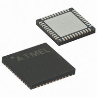
ATMEGA324P-A15MZ Atmel, ATMEGA324P-A15MZ Datasheet - Page 228

ATMEGA324P-A15MZ
Manufacturer Part Number
ATMEGA324P-A15MZ
Description
MCU AVR 32KB FLASH 15MHZ 44-VQFN
Manufacturer
Atmel
Series
AVR® ATmegar
Datasheet
1.ATMEGA324P-A15MZ.pdf
(346 pages)
Specifications of ATMEGA324P-A15MZ
Package / Case
44-VQFN Exposed Pad
Voltage - Supply (vcc/vdd)
2.7 V ~ 5.5 V
Operating Temperature
-40°C ~ 125°C
Speed
16MHz
Number Of I /o
32
Eeprom Size
1K x 8
Core Processor
AVR
Program Memory Type
FLASH
Ram Size
2K x 8
Program Memory Size
32KB (32K x 8)
Data Converters
A/D 8x10b
Oscillator Type
Internal
Peripherals
Brown-out Detect/Reset, POR, PWM, WDT
Connectivity
I²C, SPI, UART/USART
Core Size
8-Bit
Lead Free Status / RoHS Status
Lead free / RoHS Compliant
- Current page: 228 of 346
- Download datasheet (3Mb)
AVR_RESET; $C
BYPASS; $F
Boundary-scan
Related Register in I/O
Memory
MCU Control and
Status Register –
MCUCSR
228
ATmega32(L)
The active states are:
•
•
•
The AVR specific public JTAG instruction for forcing the AVR device into the Reset mode or
releasing the JTAG Reset source. The TAP controller is not reset by this instruction. The one bit
Reset Register is selected as Data Register. Note that the reset will be active as long as there is
a logic 'one' in the Reset Chain. The output from this chain is not latched.
The active states are:
•
Mandatory JTAG instruction selecting the Bypass Register for Data Register.
The active states are:
•
•
The MCU Control and Status Register contains control bits for general MCU functions, and pro-
vides information on which reset source caused an MCU Reset.
• Bit 7 – JTD: JTAG Interface Disable
When this bit is zero, the JTAG interface is enabled if the JTAGEN Fuse is programmed. If this
bit is one, the JTAG interface is disabled. In order to avoid unintentional disabling or enabling of
the JTAG interface, a timed sequence must be followed when changing this bit: The application
software must write this bit to the desired value twice within four cycles to change its value.
If the JTAG interface is left unconnected to other JTAG circuitry, the JTD bit should be set to
one. The reason for this is to avoid static current at the TDO pin in the JTAG interface.
• Bit 4 – JTRF: JTAG Reset Flag
This bit is set if a reset is being caused by a logic one in the JTAG Reset Register selected by
the JTAG instruction AVR_RESET. This bit is reset by a Power-on Reset, or by writing a logic
zero to the flag.
Bit
Read/Write
Initial Value
Capture-DR: Data on the external pins are sampled into the Boundary-scan Chain.
Shift-DR: The Boundary-scan Chain is shifted by the TCK input.
Update-DR: Data from the Boundary-scan Chain is applied to the output latches. However,
the output latches are not connected to the pins.
Shift-DR: The Reset Register is shifted by the TCK input.
Capture-DR: Loads a logic “0” into the Bypass Register.
Shift-DR: The Bypass Register cell between TDI and TDO is shifted.
JTD
R/W
7
0
ISC2
R/W
6
0
5
–
R
0
JTRF
R/W
4
WDRF
R/W
3
See Bit Description
BORF
R/W
2
EXTRF
R/W
1
PORF
R/W
0
MCUCSR
2503N–AVR–06/08
Related parts for ATMEGA324P-A15MZ
Image
Part Number
Description
Manufacturer
Datasheet
Request
R

Part Number:
Description:
Manufacturer:
Atmel Corporation
Datasheet:

Part Number:
Description:
Manufacturer:
Atmel Corporation
Datasheet:

Part Number:
Description:
IC MCU AVR 32K FLASH 44-TQFP
Manufacturer:
Atmel
Datasheet:

Part Number:
Description:
IC MCU AVR 32K FLASH 44-QFN
Manufacturer:
Atmel
Datasheet:

Part Number:
Description:
IC MCU AVR 32K FLASH 40-DIP
Manufacturer:
Atmel
Datasheet:

Part Number:
Description:
MCU AVR 32K FLASH 20MHZ 44-QFN
Manufacturer:
Atmel
Datasheet:

Part Number:
Description:
MCU AVR 32KB FLASH 20MHZ 44TQFP
Manufacturer:
Atmel
Datasheet:

Part Number:
Description:
MCU AVR 32KB FLASH 20MHZ 44QFN
Manufacturer:
Atmel
Datasheet:

Part Number:
Description:
MCU AVR 32KB FLASH 20MHZ 44TQFP
Manufacturer:
Atmel
Datasheet:

Part Number:
Description:
MCU AVR 32K FLASH 20MHZ 44-QFN
Manufacturer:
Atmel
Datasheet:

Part Number:
Description:
MCU AVR 32K FLASH 15MHZ 44-TQFP
Manufacturer:
Atmel
Datasheet:


