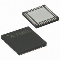
ATMEGA324P-A15MZ Atmel, ATMEGA324P-A15MZ Datasheet - Page 122

ATMEGA324P-A15MZ
Manufacturer Part Number
ATMEGA324P-A15MZ
Description
MCU AVR 32KB FLASH 15MHZ 44-VQFN
Manufacturer
Atmel
Series
AVR® ATmegar
Datasheet
1.ATMEGA324P-A15MZ.pdf
(346 pages)
Specifications of ATMEGA324P-A15MZ
Package / Case
44-VQFN Exposed Pad
Voltage - Supply (vcc/vdd)
2.7 V ~ 5.5 V
Operating Temperature
-40°C ~ 125°C
Speed
16MHz
Number Of I /o
32
Eeprom Size
1K x 8
Core Processor
AVR
Program Memory Type
FLASH
Ram Size
2K x 8
Program Memory Size
32KB (32K x 8)
Data Converters
A/D 8x10b
Oscillator Type
Internal
Peripherals
Brown-out Detect/Reset, POR, PWM, WDT
Connectivity
I²C, SPI, UART/USART
Core Size
8-Bit
Lead Free Status / RoHS Status
Lead free / RoHS Compliant
- Current page: 122 of 346
- Download datasheet (3Mb)
122
ATmega32(L)
Figure 59. Phase Correct PWM Mode, Timing Diagram
The Timer/Counter Overflow Flag (
Interrupt Flag can be used to generate an interrupt each time the counter reaches the BOTTOM
value.
In phase correct PWM mode, the compare unit allows generation of PWM waveforms on the
OC2 pin. Setting the COM21:0 bits to 2 will produce a non-inverted PWM. An inverted PWM out-
put can be generated by setting the COM21:0 to 3 (see
value will only be visible on the port pin if the data direction for the port pin is set as output. The
PWM waveform is generated by clearing (or setting) the OC2 Register at the compare match
between OCR2 and TCNT2 when the counter increments, and setting (or clearing) the OC2
Register at compare match between OCR2 and TCNT2 when the counter decrements. The
PWM frequency for the output when using phase correct PWM can be calculated by the follow-
ing equation:
The N variable represents the prescale factor (1, 8, 32, 64, 128, 256, or 1024).
The extreme values for the OCR2 Register represent special cases when generating a PWM
waveform output in the phase correct PWM mode. If the OCR2 is set equal to BOTTOM, the out-
put will be continuously low and if set equal to MAX the output will be continuously high for non-
inverted PWM mode. For inverted PWM the output will have the opposite logic values.
At the very start of period 2 in
is no Compare Match. The point of this transition is to guarantee symmetry around BOTTOM.
THere are two cases that give a transition without Compare Match.
•
•
OCR2A chages its value from MAX, like in
OCn pin value is the same as the result of a down-counting Compare Match. To ensure
symmetry around BOTTOM the OCn value at MAX must correspond to the result of an up-
counting Compare Match.
The timer starts counting from a value higher than the one in OCR2A, and for that reason
misses the Compare Match and hence the OCn change that would have happened on the
way up.
TCNTn
OCn
OCn
Period
Figure 59
1
TOV2
f
OCnPCPWM
OCn has a transition from high to low even though there
) is set each time the counter reaches BOTTOM. The
2
Figure
=
----------------- -
N 510
f
clk_I/O
⋅
59. When the OCR2A value is MAX the
Table 53 on page
3
OCn Interrupt Flag Set
OCRn Update
TOVn Interrupt Flag Set
(COMn1:0 = 2)
(COMn1:0 = 3)
126). The actual OC2
2503N–AVR–06/08
Related parts for ATMEGA324P-A15MZ
Image
Part Number
Description
Manufacturer
Datasheet
Request
R

Part Number:
Description:
Manufacturer:
Atmel Corporation
Datasheet:

Part Number:
Description:
Manufacturer:
Atmel Corporation
Datasheet:

Part Number:
Description:
IC MCU AVR 32K FLASH 44-TQFP
Manufacturer:
Atmel
Datasheet:

Part Number:
Description:
IC MCU AVR 32K FLASH 44-QFN
Manufacturer:
Atmel
Datasheet:

Part Number:
Description:
IC MCU AVR 32K FLASH 40-DIP
Manufacturer:
Atmel
Datasheet:

Part Number:
Description:
MCU AVR 32K FLASH 20MHZ 44-QFN
Manufacturer:
Atmel
Datasheet:

Part Number:
Description:
MCU AVR 32KB FLASH 20MHZ 44TQFP
Manufacturer:
Atmel
Datasheet:

Part Number:
Description:
MCU AVR 32KB FLASH 20MHZ 44QFN
Manufacturer:
Atmel
Datasheet:

Part Number:
Description:
MCU AVR 32KB FLASH 20MHZ 44TQFP
Manufacturer:
Atmel
Datasheet:

Part Number:
Description:
MCU AVR 32K FLASH 20MHZ 44-QFN
Manufacturer:
Atmel
Datasheet:

Part Number:
Description:
MCU AVR 32K FLASH 15MHZ 44-TQFP
Manufacturer:
Atmel
Datasheet:


