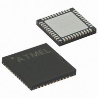
ATMEGA324P-A15MZ Atmel, ATMEGA324P-A15MZ Datasheet - Page 179

ATMEGA324P-A15MZ
Manufacturer Part Number
ATMEGA324P-A15MZ
Description
MCU AVR 32KB FLASH 15MHZ 44-VQFN
Manufacturer
Atmel
Series
AVR® ATmegar
Datasheet
1.ATMEGA324P-A15MZ.pdf
(346 pages)
Specifications of ATMEGA324P-A15MZ
Package / Case
44-VQFN Exposed Pad
Voltage - Supply (vcc/vdd)
2.7 V ~ 5.5 V
Operating Temperature
-40°C ~ 125°C
Speed
16MHz
Number Of I /o
32
Eeprom Size
1K x 8
Core Processor
AVR
Program Memory Type
FLASH
Ram Size
2K x 8
Program Memory Size
32KB (32K x 8)
Data Converters
A/D 8x10b
Oscillator Type
Internal
Peripherals
Brown-out Detect/Reset, POR, PWM, WDT
Connectivity
I²C, SPI, UART/USART
Core Size
8-Bit
Lead Free Status / RoHS Status
Lead free / RoHS Compliant
- Current page: 179 of 346
- Download datasheet (3Mb)
TWI Data Register –
TWDR
TWI (Slave) Address
Register – TWAR
2503N–AVR–06/08
• Bits 1..0 – TWPS: TWI Prescaler Bits
These bits can be read and written, and control the bit rate prescaler.
Table 73. TWI Bit Rate Prescaler
To calculate bit rates, see
used in the equation.
In Transmit mode, TWDR contains the next byte to be transmitted. In Receive mode, the TWDR
contains the last byte received. It is writable while the TWI is not in the process of shifting a byte.
This occurs when the TWI Interrupt Flag (TWINT) is set by hardware. Note that the Data Regis-
ter cannot be initialized by the user before the first interrupt occurs. The data in TWDR remains
stable as long as TWINT is set. While data is shifted out, data on the bus is simultaneously
shifted in. TWDR always contains the last byte present on the bus, except after a wake up from
a sleep mode by the TWI interrupt. In this case, the contents of TWDR is undefined. In the case
of a lost bus arbitration, no data is lost in the transition from Master to Slave. Handling of the
ACK bit is controlled automatically by the TWI logic, the CPU cannot access the ACK bit directly.
• Bits 7..0 – TWD: TWI Data Register
These eight bits contin the next data byte to be transmitted, or the latest data byte received on
the Two-wire Serial Bus.
The TWAR should be loaded with the 7-bit slave address (in the seven most significant bits of
TWAR) to which the TWI will respond when programmed as a slave transmitter or receiver. In
multimaster systems, TWAR must be set in masters which can be addressed as slaves by other
masters.
The LSB of TWAR is used to enable recognition of the general call address ($00). There is an
associated address comparator that looks for the slave address (or general call address if
enabled) in the received serial address. If a match is found, an interrupt request is generated.
• Bits 7..1 – TWA: TWI (Slave) Address Register
These seven bits constitute the slave address of the TWI unit.
Bit
Read/Write
Initial Value
Bit
Read/Write
Initial Value
TWPS1
0
0
1
1
TWD7
TWA6
R/W
R/W
7
1
7
1
TWD6
TWA5
R/W
R/W
6
1
6
1
“Bit Rate Generator Unit” on page
TWD5
TWA4
TWPS0
R/W
R/W
5
1
5
1
0
1
0
1
TWD4
TWA3
R/W
R/W
4
1
4
1
Prescaler Value
1
4
16
64
TWD3
TWA2
R/W
R/W
3
1
3
1
TWD2
TWA1
R/W
R/W
2
1
2
1
TWD1
TWA0
175. The value of TWPS1..0 is
R/W
R/W
1
1
1
1
ATmega32(L)
TWGCE
TWD0
R/W
R/W
0
1
0
0
TWDR
TWAR
179
Related parts for ATMEGA324P-A15MZ
Image
Part Number
Description
Manufacturer
Datasheet
Request
R

Part Number:
Description:
Manufacturer:
Atmel Corporation
Datasheet:

Part Number:
Description:
Manufacturer:
Atmel Corporation
Datasheet:

Part Number:
Description:
IC MCU AVR 32K FLASH 44-TQFP
Manufacturer:
Atmel
Datasheet:

Part Number:
Description:
IC MCU AVR 32K FLASH 44-QFN
Manufacturer:
Atmel
Datasheet:

Part Number:
Description:
IC MCU AVR 32K FLASH 40-DIP
Manufacturer:
Atmel
Datasheet:

Part Number:
Description:
MCU AVR 32K FLASH 20MHZ 44-QFN
Manufacturer:
Atmel
Datasheet:

Part Number:
Description:
MCU AVR 32KB FLASH 20MHZ 44TQFP
Manufacturer:
Atmel
Datasheet:

Part Number:
Description:
MCU AVR 32KB FLASH 20MHZ 44QFN
Manufacturer:
Atmel
Datasheet:

Part Number:
Description:
MCU AVR 32KB FLASH 20MHZ 44TQFP
Manufacturer:
Atmel
Datasheet:

Part Number:
Description:
MCU AVR 32K FLASH 20MHZ 44-QFN
Manufacturer:
Atmel
Datasheet:

Part Number:
Description:
MCU AVR 32K FLASH 15MHZ 44-TQFP
Manufacturer:
Atmel
Datasheet:


