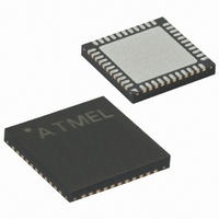
ATMEGA324P-A15MZ Atmel, ATMEGA324P-A15MZ Datasheet - Page 141

ATMEGA324P-A15MZ
Manufacturer Part Number
ATMEGA324P-A15MZ
Description
MCU AVR 32KB FLASH 15MHZ 44-VQFN
Manufacturer
Atmel
Series
AVR® ATmegar
Datasheet
1.ATMEGA324P-A15MZ.pdf
(346 pages)
Specifications of ATMEGA324P-A15MZ
Package / Case
44-VQFN Exposed Pad
Voltage - Supply (vcc/vdd)
2.7 V ~ 5.5 V
Operating Temperature
-40°C ~ 125°C
Speed
16MHz
Number Of I /o
32
Eeprom Size
1K x 8
Core Processor
AVR
Program Memory Type
FLASH
Ram Size
2K x 8
Program Memory Size
32KB (32K x 8)
Data Converters
A/D 8x10b
Oscillator Type
Internal
Peripherals
Brown-out Detect/Reset, POR, PWM, WDT
Connectivity
I²C, SPI, UART/USART
Core Size
8-Bit
Lead Free Status / RoHS Status
Lead free / RoHS Compliant
- Current page: 141 of 346
- Download datasheet (3Mb)
AVR USART vs. AVR
UART – Compatibility
Clock Generation
2503N–AVR–06/08
The dashed boxes in the block diagram separate the three main parts of the USART (listed from
the top): Clock Generator, Transmitter and Receiver. Control Registers are shared by all units.
The clock generation logic consists of synchronization logic for external clock input used by syn-
chronous slave operation, and the baud rate generator. The XCK (Transfer Clock) pin is only
used by Synchronous Transfer mode. The Transmitter consists of a single write buffer, a serial
Shift Register, parity generator and control logic for handling different serial frame formats. The
write buffer allows a continuous transfer of data without any delay between frames. The
Receiver is the most complex part of the USART module due to its clock and data recovery
units. The recovery units are used for asynchronous data reception. In addition to the recovery
units, the receiver includes a parity checker, control logic, a Shift Register and a two level
receive buffer (UDR). The receiver supports the same frame formats as the transmitter, and can
detect frame error, data overrun and parity errors.
The USART is fully compatible with the AVR UART regarding:
•
•
•
•
•
However, the receive buffering has two improvements that will affect the compatibility in some
special cases:
•
•
The following control bits have changed name, but have same functionality and register location:
•
•
The clock generation logic generates the base clock for the Transmitter and Receiver. The
USART supports four modes of clock operation: Normal Asynchronous, Double Speed Asyn-
chronous, Master Synchronous and Slave Synchronous mode. The UMSEL bit in USART
Control and Status Register C (UCSRC) selects between asynchronous and synchronous oper-
ation. Double Speed (Asynchronous mode only) is controlled by the U2X found in the UCSRA
Register. When using Synchronous mode (UMSEL = 1), the Data Direction Register for the XCK
pin (DDR_XCK) controls whether the clock source is internal (Master mode) or external (Slave
mode). The XCK pin is only active when using Synchronous mode.
Figure 70
Bit locations inside all USART Registers
Baud Rate Generation
Transmitter Operation
Transmit Buffer Functionality
Receiver Operation
A second Buffer Register has been added. The two Buffer Registers operate as a circular
FIFO buffer. Therefore the UDR must only be read once for each incoming data! More
important is the fact that the Error Flags (FE and DOR) and the 9th data bit (RXB8) are
buffered with the data in the receive buffer. Therefore the status bits must always be read
before the UDR Register is read. Otherwise the error status will be lost since the buffer state
is lost.
The receiver Shift Register can now act as a third buffer level. This is done by allowing the
received data to remain in the serial Shift Register (see
full, until a new start bit is detected. The USART is therefore more resistant to Data OverRun
(DOR) error conditions.
CHR9 is changed to UCSZ2
OR is changed to DOR
shows a block diagram of the clock generation logic.
Figure
69) if the Buffer Registers are
ATmega32(L)
141
Related parts for ATMEGA324P-A15MZ
Image
Part Number
Description
Manufacturer
Datasheet
Request
R

Part Number:
Description:
Manufacturer:
Atmel Corporation
Datasheet:

Part Number:
Description:
Manufacturer:
Atmel Corporation
Datasheet:

Part Number:
Description:
IC MCU AVR 32K FLASH 44-TQFP
Manufacturer:
Atmel
Datasheet:

Part Number:
Description:
IC MCU AVR 32K FLASH 44-QFN
Manufacturer:
Atmel
Datasheet:

Part Number:
Description:
IC MCU AVR 32K FLASH 40-DIP
Manufacturer:
Atmel
Datasheet:

Part Number:
Description:
MCU AVR 32K FLASH 20MHZ 44-QFN
Manufacturer:
Atmel
Datasheet:

Part Number:
Description:
MCU AVR 32KB FLASH 20MHZ 44TQFP
Manufacturer:
Atmel
Datasheet:

Part Number:
Description:
MCU AVR 32KB FLASH 20MHZ 44QFN
Manufacturer:
Atmel
Datasheet:

Part Number:
Description:
MCU AVR 32KB FLASH 20MHZ 44TQFP
Manufacturer:
Atmel
Datasheet:

Part Number:
Description:
MCU AVR 32K FLASH 20MHZ 44-QFN
Manufacturer:
Atmel
Datasheet:

Part Number:
Description:
MCU AVR 32K FLASH 15MHZ 44-TQFP
Manufacturer:
Atmel
Datasheet:


