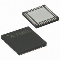
ATMEGA324P-A15MZ Atmel, ATMEGA324P-A15MZ Datasheet - Page 273

ATMEGA324P-A15MZ
Manufacturer Part Number
ATMEGA324P-A15MZ
Description
MCU AVR 32KB FLASH 15MHZ 44-VQFN
Manufacturer
Atmel
Series
AVR® ATmegar
Datasheet
1.ATMEGA324P-A15MZ.pdf
(346 pages)
Specifications of ATMEGA324P-A15MZ
Package / Case
44-VQFN Exposed Pad
Voltage - Supply (vcc/vdd)
2.7 V ~ 5.5 V
Operating Temperature
-40°C ~ 125°C
Speed
16MHz
Number Of I /o
32
Eeprom Size
1K x 8
Core Processor
AVR
Program Memory Type
FLASH
Ram Size
2K x 8
Program Memory Size
32KB (32K x 8)
Data Converters
A/D 8x10b
Oscillator Type
Internal
Peripherals
Brown-out Detect/Reset, POR, PWM, WDT
Connectivity
I²C, SPI, UART/USART
Core Size
8-Bit
Lead Free Status / RoHS Status
Lead free / RoHS Compliant
- Current page: 273 of 346
- Download datasheet (3Mb)
Table 115. SPI Serial Programming Instruction Set
Note:
2503N–AVR–06/08
Instruction
Programming Enable
Chip Erase
Read Program Memory
Load Program Memory Page
Write Program Memory Page
Read EEPROM Memory
Write EEPROM Memory
Read Lock Bits
Write Lock Bits
Read Signature Byte
Write Fuse Bits
Write Fuse High Bits
Read Fuse Bits
Read Fuse High Bits
Read Calibration Byte
a = address high bits
b = address low bits
H = 0 – Low byte, 1 – High Byte
o = data out
i = data in
x = don’t care
1010 1100
1010 1100
0010 H000
0100 H000
0100 1100
1010 0000
1100 0000
0101 1000
1010 1100
0011 0000
1010 1100
1010 1100
0101 0000
0101 1000
0011 1000
Byte 1
0101 0011
100x xxxx
00aa aaaa
00xx xxxx
00aa aaaa
00xx xxaa
00xx xxaa
0000 0000
111x xxxx
00xx xxxx
1010 0000
1010 1000
0000 0000
0000 1000
xxxx xxxx
Byte 2
Instruction Format
xxxx xxxx
xxxx xxxx
bbbb bbbb
xxbb bbbb
bbxx xxxx
bbbb bbbb
bbbb bbbb
xxxx xxxx
xxxx xxxx
xxxx xxbb
xxxx xxxx
xxxx xxxx
xxxx xxxx
xxxx xxxx
0000 00bb
Byte 3
xxxx xxxx
xxxx xxxx
oooo oooo
iiii iiii
xxxx xxxx
oooo oooo
iiii iiii
xxoo oooo
11ii iiii
oooo oooo
iiii iiii
iiii iiii
oooo oooo
oooo oooo
oooo oooo
Byte4
Operation
Enable SPI Serial Programming after
RESET goes low.
Chip Erase EEPROM and Flash.
Read H (high or low) data o from
Program memory at word address a:b.
Write H (high or low) data i to Program
Memory page at word address b. Data
low byte must be loaded before Data
high byte is applied within the same
address.
Write Program Memory Page at
address a:b.
Read data o from EEPROM memory at
address a:b.
Write data i to EEPROM memory at
address a:b.
Read Lock bits. “0” = programmed, “1”
= unprogrammed. See
page 256
Write Lock bits. Set bits = “0” to
program Lock bits. See
page 256
Read Signature Byte o at address b.
Set bits = “0” to program, “1” to
unprogram. See
258
Set bits = “0” to program, “1” to
unprogram. See
257
Read Fuse bits. “0” = programmed, “1”
= unprogrammed. See
page 258
Read Fuse high bits. “0” = pro-
grammed, “1” = unprogrammed. See
Table 104 on page 257
Read Calibration Byte o at address b
for details.
for details.
for details.
for details.
for details.
ATmega32(L)
Table 105 on page
Table 104 on page
Table 102 on
Table 105 on
Table 102 on
for details.
273
Related parts for ATMEGA324P-A15MZ
Image
Part Number
Description
Manufacturer
Datasheet
Request
R

Part Number:
Description:
Manufacturer:
Atmel Corporation
Datasheet:

Part Number:
Description:
Manufacturer:
Atmel Corporation
Datasheet:

Part Number:
Description:
IC MCU AVR 32K FLASH 44-TQFP
Manufacturer:
Atmel
Datasheet:

Part Number:
Description:
IC MCU AVR 32K FLASH 44-QFN
Manufacturer:
Atmel
Datasheet:

Part Number:
Description:
IC MCU AVR 32K FLASH 40-DIP
Manufacturer:
Atmel
Datasheet:

Part Number:
Description:
MCU AVR 32K FLASH 20MHZ 44-QFN
Manufacturer:
Atmel
Datasheet:

Part Number:
Description:
MCU AVR 32KB FLASH 20MHZ 44TQFP
Manufacturer:
Atmel
Datasheet:

Part Number:
Description:
MCU AVR 32KB FLASH 20MHZ 44QFN
Manufacturer:
Atmel
Datasheet:

Part Number:
Description:
MCU AVR 32KB FLASH 20MHZ 44TQFP
Manufacturer:
Atmel
Datasheet:

Part Number:
Description:
MCU AVR 32K FLASH 20MHZ 44-QFN
Manufacturer:
Atmel
Datasheet:

Part Number:
Description:
MCU AVR 32K FLASH 15MHZ 44-TQFP
Manufacturer:
Atmel
Datasheet:


