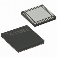
ATMEGA324P-A15MZ Atmel, ATMEGA324P-A15MZ Datasheet - Page 128

ATMEGA324P-A15MZ
Manufacturer Part Number
ATMEGA324P-A15MZ
Description
MCU AVR 32KB FLASH 15MHZ 44-VQFN
Manufacturer
Atmel
Series
AVR® ATmegar
Datasheet
1.ATMEGA324P-A15MZ.pdf
(346 pages)
Specifications of ATMEGA324P-A15MZ
Package / Case
44-VQFN Exposed Pad
Voltage - Supply (vcc/vdd)
2.7 V ~ 5.5 V
Operating Temperature
-40°C ~ 125°C
Speed
16MHz
Number Of I /o
32
Eeprom Size
1K x 8
Core Processor
AVR
Program Memory Type
FLASH
Ram Size
2K x 8
Program Memory Size
32KB (32K x 8)
Data Converters
A/D 8x10b
Oscillator Type
Internal
Peripherals
Brown-out Detect/Reset, POR, PWM, WDT
Connectivity
I²C, SPI, UART/USART
Core Size
8-Bit
Lead Free Status / RoHS Status
Lead free / RoHS Compliant
- Current page: 128 of 346
- Download datasheet (3Mb)
Asynchronous
Operation of the
Timer/Counter
Asynchronous Status
Register – ASSR
Asynchronous
Operation of
Timer/Counter2
128
ATmega32(L)
• Bit 3 – AS2: Asynchronous Timer/Counter2
When AS2 is written to zero, Timer/Counter 2 is clocked from the I/O clock, clk
written to one, Timer/Counter2 is clocked from a Crystal Oscillator connected to the Timer Oscil-
lator 1 (TOSC1) pin. When the value of AS2 is changed, the contents of TCNT2, OCR2, and
TCCR2 might be corrupted.
• Bit 2 – TCN2UB: Timer/Counter2 Update Busy
When Timer/Counter2 operates asynchronously and TCNT2 is written, this bit becomes set.
When TCNT2 has been updated from the temporary storage register, this bit is cleared by hard-
ware. A logical zero in this bit indicates that TCNT2 is ready to be updated with a new value.
• Bit 1 – OCR2UB: Output Compare Register2 Update Busy
When Timer/Counter2 operates asynchronously and OCR2 is written, this bit becomes set.
When OCR2 has been updated from the temporary storage register, this bit is cleared by hard-
ware. A logical zero in this bit indicates that OCR2 is ready to be updated with a new value.
• Bit 0 – TCR2UB: Timer/Counter Control Register2 Update Busy
When Timer/Counter2 operates asynchronously and TCCR2 is written, this bit becomes set.
When TCCR2 has been updated from the temporary storage register, this bit is cleared by hard-
ware. A logical zero in this bit indicates that TCCR2 is ready to be updated with a new value.
If a write is performed to any of the three Timer/Counter2 Registers while its update busy flag is
set, the updated value might get corrupted and cause an unintentional interrupt to occur.
The mechanisms for reading TCNT2, OCR2, and TCCR2 are different. When reading TCNT2,
the actual timer value is read. When reading OCR2 or TCCR2, the value in the temporary stor-
age register is read.
When Timer/Counter2 operates asynchronously, some considerations must be taken.
•
Bit
Read/Write
Initial Value
Warning: When switching between asynchronous and synchronous clocking of
Timer/Counter2, the Timer Registers TCNT2, OCR2, and TCCR2 might be corrupted. A
safe procedure for switching clock source is:
1. Disable the Timer/Counter2 interrupts by clearing OCIE2 and TOIE2.
2. Select clock source by setting AS2 as appropriate.
3. Write new values to TCNT2, OCR2, and TCCR2.
4. To switch to asynchronous operation: Wait for TCN2UB, OCR2UB, and TCR2UB.
5. Clear the Timer/Counter2 Interrupt Flags.
6. Enable interrupts, if needed.
R
7
–
0
R
6
–
0
R
5
–
0
R
4
–
0
AS2
R/W
3
0
TCN2UB
R
2
0
OCR2UB
R
1
0
TCR2UB
R
0
0
I/O
ASSR
. When AS2 is
2503N–AVR–06/08
Related parts for ATMEGA324P-A15MZ
Image
Part Number
Description
Manufacturer
Datasheet
Request
R

Part Number:
Description:
Manufacturer:
Atmel Corporation
Datasheet:

Part Number:
Description:
Manufacturer:
Atmel Corporation
Datasheet:

Part Number:
Description:
IC MCU AVR 32K FLASH 44-TQFP
Manufacturer:
Atmel
Datasheet:

Part Number:
Description:
IC MCU AVR 32K FLASH 44-QFN
Manufacturer:
Atmel
Datasheet:

Part Number:
Description:
IC MCU AVR 32K FLASH 40-DIP
Manufacturer:
Atmel
Datasheet:

Part Number:
Description:
MCU AVR 32K FLASH 20MHZ 44-QFN
Manufacturer:
Atmel
Datasheet:

Part Number:
Description:
MCU AVR 32KB FLASH 20MHZ 44TQFP
Manufacturer:
Atmel
Datasheet:

Part Number:
Description:
MCU AVR 32KB FLASH 20MHZ 44QFN
Manufacturer:
Atmel
Datasheet:

Part Number:
Description:
MCU AVR 32KB FLASH 20MHZ 44TQFP
Manufacturer:
Atmel
Datasheet:

Part Number:
Description:
MCU AVR 32K FLASH 20MHZ 44-QFN
Manufacturer:
Atmel
Datasheet:

Part Number:
Description:
MCU AVR 32K FLASH 15MHZ 44-TQFP
Manufacturer:
Atmel
Datasheet:


