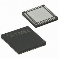
ATMEGA324P-A15MZ Atmel, ATMEGA324P-A15MZ Datasheet - Page 63

ATMEGA324P-A15MZ
Manufacturer Part Number
ATMEGA324P-A15MZ
Description
MCU AVR 32KB FLASH 15MHZ 44-VQFN
Manufacturer
Atmel
Series
AVR® ATmegar
Datasheet
1.ATMEGA324P-A15MZ.pdf
(346 pages)
Specifications of ATMEGA324P-A15MZ
Package / Case
44-VQFN Exposed Pad
Voltage - Supply (vcc/vdd)
2.7 V ~ 5.5 V
Operating Temperature
-40°C ~ 125°C
Speed
16MHz
Number Of I /o
32
Eeprom Size
1K x 8
Core Processor
AVR
Program Memory Type
FLASH
Ram Size
2K x 8
Program Memory Size
32KB (32K x 8)
Data Converters
A/D 8x10b
Oscillator Type
Internal
Peripherals
Brown-out Detect/Reset, POR, PWM, WDT
Connectivity
I²C, SPI, UART/USART
Core Size
8-Bit
Lead Free Status / RoHS Status
Lead free / RoHS Compliant
- Current page: 63 of 346
- Download datasheet (3Mb)
2503N–AVR–06/08
• OC1A – Port D, Bit 5
OC1A, Output Compare Match A output: The PD5 pin can serve as an external output for the
Timer/Counter1 Output Compare A. The pin has to be configured as an output (DDD5 set (one))
to serve this function. The OC1A pin is also the output pin for the PWM mode timer function.
• OC1B – Port D, Bit 4
OC1B, Output Compare Match B output: The PD4 pin can serve as an external output for the
Timer/Counter1 Output Compare B. The pin has to be configured as an output (DDD4 set (one))
to serve this function. The OC1B pin is also the output pin for the PWM mode timer function.
• INT1 – Port D, Bit 3
INT1, External Interrupt Source 1: The PD3 pin can serve as an external interrupt source.
• INT0 – Port D, Bit 2
INT0, External Interrupt Source 0: The PD2 pin can serve as an external interrupt source.
• TXD – Port D, Bit 1
TXD, Transmit Data (Data output pin for the USART). When the USART Transmitter is enabled,
this pin is configured as an output regardless of the value of DDD1.
• RXD – Port D, Bit 0
RXD, Receive Data (Data input pin for the USART). When the USART Receiver is enabled this
pin is configured as an input regardless of the value of DDD0. When the USART forces this pin
to be an input, the pull-up can still be controlled by the PORTD0 bit.
Table 32
Figure 26 on page
Table 32. Overriding Signals for Alternate Functions PD7..PD4
Signal Name
PUOE
PUOV
DDOE
DDOV
PVOE
PVOV
DIEOE
DIEOV
DI
AIO
and
Table 33
PD7/OC2
0
0
0
0
OC2 ENABLE
OC2
0
0
–
–
54.
relate the alternate functions of Port D to the overriding signals shown in
ICP1 INPUT
PD6/ICP1
0
0
0
0
0
0
0
0
–
PD5/OC1A
0
0
0
0
OC1A ENABLE
OC1A
0
0
–
–
PD4/OC1B
0
0
0
0
OC1B ENABLE
OC1B
0
0
–
–
ATmega32(L)
63
Related parts for ATMEGA324P-A15MZ
Image
Part Number
Description
Manufacturer
Datasheet
Request
R

Part Number:
Description:
Manufacturer:
Atmel Corporation
Datasheet:

Part Number:
Description:
Manufacturer:
Atmel Corporation
Datasheet:

Part Number:
Description:
IC MCU AVR 32K FLASH 44-TQFP
Manufacturer:
Atmel
Datasheet:

Part Number:
Description:
IC MCU AVR 32K FLASH 44-QFN
Manufacturer:
Atmel
Datasheet:

Part Number:
Description:
IC MCU AVR 32K FLASH 40-DIP
Manufacturer:
Atmel
Datasheet:

Part Number:
Description:
MCU AVR 32K FLASH 20MHZ 44-QFN
Manufacturer:
Atmel
Datasheet:

Part Number:
Description:
MCU AVR 32KB FLASH 20MHZ 44TQFP
Manufacturer:
Atmel
Datasheet:

Part Number:
Description:
MCU AVR 32KB FLASH 20MHZ 44QFN
Manufacturer:
Atmel
Datasheet:

Part Number:
Description:
MCU AVR 32KB FLASH 20MHZ 44TQFP
Manufacturer:
Atmel
Datasheet:

Part Number:
Description:
MCU AVR 32K FLASH 20MHZ 44-QFN
Manufacturer:
Atmel
Datasheet:

Part Number:
Description:
MCU AVR 32K FLASH 15MHZ 44-TQFP
Manufacturer:
Atmel
Datasheet:


