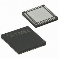
ATMEGA324P-A15MZ Atmel, ATMEGA324P-A15MZ Datasheet - Page 97

ATMEGA324P-A15MZ
Manufacturer Part Number
ATMEGA324P-A15MZ
Description
MCU AVR 32KB FLASH 15MHZ 44-VQFN
Manufacturer
Atmel
Series
AVR® ATmegar
Datasheet
1.ATMEGA324P-A15MZ.pdf
(346 pages)
Specifications of ATMEGA324P-A15MZ
Package / Case
44-VQFN Exposed Pad
Voltage - Supply (vcc/vdd)
2.7 V ~ 5.5 V
Operating Temperature
-40°C ~ 125°C
Speed
16MHz
Number Of I /o
32
Eeprom Size
1K x 8
Core Processor
AVR
Program Memory Type
FLASH
Ram Size
2K x 8
Program Memory Size
32KB (32K x 8)
Data Converters
A/D 8x10b
Oscillator Type
Internal
Peripherals
Brown-out Detect/Reset, POR, PWM, WDT
Connectivity
I²C, SPI, UART/USART
Core Size
8-Bit
Lead Free Status / RoHS Status
Lead free / RoHS Compliant
- Current page: 97 of 346
- Download datasheet (3Mb)
Compare Output Mode
and Waveform
Generation
Modes of
Operation
2503N–AVR–06/08
Figure 44. Compare Match Output Unit, Schematic
The general I/O port function is overridden by the Output Compare (OC1x) from the Waveform
Generator if either of the COM1x1:0 bits are set. However, the OC1x pin direction (input or out-
put) is still controlled by the Data Direction Register (DDR) for the port pin. The Data Direction
Register bit for the OC1x pin (DDR_OC1x) must be set as output before the OC1x value is visi-
ble on the pin. The port override function is generally independent of the Waveform Generation
mode, but there are some exceptions. Refer to
The design of the output compare pin logic allows initialization of the OC1x state before the out-
put is enabled. Note that some COM1x1:0 bit settings are reserved for certain modes of
operation.
The COM1x1:0 bits have no effect on the Input Capture unit.
The Waveform Generator uses the COM1x1:0 bits differently in normal, CTC, and PWM modes.
For all modes, setting the COM1x1:0 = 0 tells the Waveform Generator that no action on the
OC1x Register is to be performed on the next compare match. For compare output actions in the
non-PWM modes refer to
108, and for phase correct and phase and frequency correct PWM refer to
108.
A change of the COM1x1:0 bits state will have effect at the first compare match after the bits are
written. For non-PWM modes, the action can be forced to have immediate effect by using the
FOC1x strobe bits.
The mode of operation, i.e., the behavior of the Timer/Counter and the output compare pins, is
defined by the combination of the Waveform Generation mode (WGM13:0) and Compare Output
mode (COM1x1:0) bits. The Compare Output mode bits do not affect the counting sequence,
while the Waveform Generation mode bits do. The COM1x1:0 bits control whether the PWM out-
put generated should be inverted or not (inverted or non-inverted PWM). For non-PWM modes
the COM1x1:0 bits control whether the output should be set, cleared or toggle at a compare
match
For detailed timing information refer to
(See “Compare Match Output Unit” on page
See “16-bit Timer/Counter Register Description” on page 107.
COMnx1
COMnx0
FOCnx
clk
I/O
Table 44 on page
Waveform
Generator
“Timer/Counter Timing Diagrams” on page
D
D
D
PORT
DDR
OCnx
107. For fast PWM mode refer to
Table
Q
Q
Q
96.)
44,
Table 45
1
0
and
ATmega32(L)
Table 46
OCnx
Pin
Table 46 on page
Table 45 on page
for details.
105.
97
Related parts for ATMEGA324P-A15MZ
Image
Part Number
Description
Manufacturer
Datasheet
Request
R

Part Number:
Description:
Manufacturer:
Atmel Corporation
Datasheet:

Part Number:
Description:
Manufacturer:
Atmel Corporation
Datasheet:

Part Number:
Description:
IC MCU AVR 32K FLASH 44-TQFP
Manufacturer:
Atmel
Datasheet:

Part Number:
Description:
IC MCU AVR 32K FLASH 44-QFN
Manufacturer:
Atmel
Datasheet:

Part Number:
Description:
IC MCU AVR 32K FLASH 40-DIP
Manufacturer:
Atmel
Datasheet:

Part Number:
Description:
MCU AVR 32K FLASH 20MHZ 44-QFN
Manufacturer:
Atmel
Datasheet:

Part Number:
Description:
MCU AVR 32KB FLASH 20MHZ 44TQFP
Manufacturer:
Atmel
Datasheet:

Part Number:
Description:
MCU AVR 32KB FLASH 20MHZ 44QFN
Manufacturer:
Atmel
Datasheet:

Part Number:
Description:
MCU AVR 32KB FLASH 20MHZ 44TQFP
Manufacturer:
Atmel
Datasheet:

Part Number:
Description:
MCU AVR 32K FLASH 20MHZ 44-QFN
Manufacturer:
Atmel
Datasheet:

Part Number:
Description:
MCU AVR 32K FLASH 15MHZ 44-TQFP
Manufacturer:
Atmel
Datasheet:


