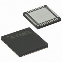
ATMEGA324P-A15MZ Atmel, ATMEGA324P-A15MZ Datasheet - Page 248

ATMEGA324P-A15MZ
Manufacturer Part Number
ATMEGA324P-A15MZ
Description
MCU AVR 32KB FLASH 15MHZ 44-VQFN
Manufacturer
Atmel
Series
AVR® ATmegar
Datasheet
1.ATMEGA324P-A15MZ.pdf
(346 pages)
Specifications of ATMEGA324P-A15MZ
Package / Case
44-VQFN Exposed Pad
Voltage - Supply (vcc/vdd)
2.7 V ~ 5.5 V
Operating Temperature
-40°C ~ 125°C
Speed
16MHz
Number Of I /o
32
Eeprom Size
1K x 8
Core Processor
AVR
Program Memory Type
FLASH
Ram Size
2K x 8
Program Memory Size
32KB (32K x 8)
Data Converters
A/D 8x10b
Oscillator Type
Internal
Peripherals
Brown-out Detect/Reset, POR, PWM, WDT
Connectivity
I²C, SPI, UART/USART
Core Size
8-Bit
Lead Free Status / RoHS Status
Lead free / RoHS Compliant
- Current page: 248 of 346
- Download datasheet (3Mb)
Store Program
Memory Control
Register – SPMCR
248
ATmega32(L)
Table 97. Boot Reset Fuse
Note:
The Store Program Memory Control Register contains the control bits needed to control the Boot
Loader operations.
• Bit 7 – SPMIE: SPM Interrupt Enable
When the SPMIE bit is written to one, and the I-bit in the Status Register is set (one), the SPM
ready interrupt will be enabled. The SPM ready Interrupt will be executed as long as the SPMEN
bit in the SPMCR Register is cleared.
• Bit 6 – RWWSB: Read-While-Write Section Busy
When a self-programming (Page Erase or Page Write) operation to the RWW section is initiated,
the RWWSB will be set (one) by hardware. When the RWWSB bit is set, the RWW section can-
not be accessed. The RWWSB bit will be cleared if the RWWSRE bit is written to one after a
Self-Programming operation is completed. Alternatively the RWWSB bit will automatically be
cleared if a page load operation is initiated.
• Bit 5 – Res: Reserved Bit
This bit is a reserved bit in the ATmega32 and always read as zero.
• Bit 4 – RWWSRE: Read-While-Write Section Read Enable
When programming (Page Erase or Page Write) to the RWW section, the RWW section is
blocked for reading (the RWWSB will be set by hardware). To re-enable the RWW section, the
user software must wait until the programming is completed (SPMEN will be cleared). Then, if
the RWWSRE bit is written to one at the same time as SPMEN, the next SPM instruction within
four clock cycles re-enables the RWW section. The RWW section cannot be re-enabled while
the Flash is busy with a page erase or a page write (SPMEN is set). If the RWWSRE bit is writ-
ten while the Flash is being loaded, the Flash load operation will abort and the data loaded will
be lost.
• Bit 3 – BLBSET: Boot Lock Bit Set
If this bit is written to one at the same time as SPMEN, the next SPM instruction within four clock
cycles sets Boot Lock bits, according to the data in R0. The data in R1 and the address in the Z-
pointer are ignored. The BLBSET bit will automatically be cleared upon completion of the Lock
bit set, or if no SPM instruction is executed within four clock cycles.
An LPM instruction within three cycles after BLBSET and SPMEN are set in the SPMCR Regis-
ter, will read either the Lock bits or the Fuse bits (depending on Z0 in the Z-pointer) into the
destination register. See
details.
Bit
Read/Write
Initial value
BOOTRST
1
0
1. “1” means unprogrammed, “0” means programmed
SPMIE
R/W
7
0
Reset Address
Reset Vector = Application reset (address $0000)
Reset Vector = Boot Loader reset (see
RWWSB
R
6
0
“Reading the Fuse and Lock Bits from Software” on page 252
(1)
R
5
–
0
RWWSRE
R/W
4
0
BLBSET
R/W
3
0
Table 99 on page
PGWRT
R/W
2
0
PGERS
R/W
1
0
255)
SPMEN
R/W
0
0
SPMCR
2503N–AVR–06/08
for
Related parts for ATMEGA324P-A15MZ
Image
Part Number
Description
Manufacturer
Datasheet
Request
R

Part Number:
Description:
Manufacturer:
Atmel Corporation
Datasheet:

Part Number:
Description:
Manufacturer:
Atmel Corporation
Datasheet:

Part Number:
Description:
IC MCU AVR 32K FLASH 44-TQFP
Manufacturer:
Atmel
Datasheet:

Part Number:
Description:
IC MCU AVR 32K FLASH 44-QFN
Manufacturer:
Atmel
Datasheet:

Part Number:
Description:
IC MCU AVR 32K FLASH 40-DIP
Manufacturer:
Atmel
Datasheet:

Part Number:
Description:
MCU AVR 32K FLASH 20MHZ 44-QFN
Manufacturer:
Atmel
Datasheet:

Part Number:
Description:
MCU AVR 32KB FLASH 20MHZ 44TQFP
Manufacturer:
Atmel
Datasheet:

Part Number:
Description:
MCU AVR 32KB FLASH 20MHZ 44QFN
Manufacturer:
Atmel
Datasheet:

Part Number:
Description:
MCU AVR 32KB FLASH 20MHZ 44TQFP
Manufacturer:
Atmel
Datasheet:

Part Number:
Description:
MCU AVR 32K FLASH 20MHZ 44-QFN
Manufacturer:
Atmel
Datasheet:

Part Number:
Description:
MCU AVR 32K FLASH 15MHZ 44-TQFP
Manufacturer:
Atmel
Datasheet:


