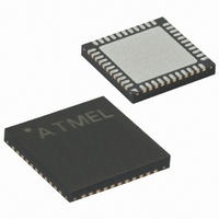
ATMEGA324P-A15MZ Atmel, ATMEGA324P-A15MZ Datasheet - Page 66

ATMEGA324P-A15MZ
Manufacturer Part Number
ATMEGA324P-A15MZ
Description
MCU AVR 32KB FLASH 15MHZ 44-VQFN
Manufacturer
Atmel
Series
AVR® ATmegar
Datasheet
1.ATMEGA324P-A15MZ.pdf
(346 pages)
Specifications of ATMEGA324P-A15MZ
Package / Case
44-VQFN Exposed Pad
Voltage - Supply (vcc/vdd)
2.7 V ~ 5.5 V
Operating Temperature
-40°C ~ 125°C
Speed
16MHz
Number Of I /o
32
Eeprom Size
1K x 8
Core Processor
AVR
Program Memory Type
FLASH
Ram Size
2K x 8
Program Memory Size
32KB (32K x 8)
Data Converters
A/D 8x10b
Oscillator Type
Internal
Peripherals
Brown-out Detect/Reset, POR, PWM, WDT
Connectivity
I²C, SPI, UART/USART
Core Size
8-Bit
Lead Free Status / RoHS Status
Lead free / RoHS Compliant
- Current page: 66 of 346
- Download datasheet (3Mb)
External
Interrupts
MCU Control Register
– MCUCR
66
ATmega32(L)
The External Interrupts are triggered by the INT0, INT1, and INT2 pins. Observe that, if enabled,
the interrupts will trigger even if the INT0..2 pins are configured as outputs. This feature provides
a way of generating a software interrupt. The external interrupts can be triggered by a falling or
rising edge or a low level (INT2 is only an edge triggered interrupt). This is set up as indicated in
the specification for the MCU Control Register – MCUCR – and MCU Control and Status Regis-
ter – MCUCSR. When the external interrupt is enabled and is configured as level triggered (only
INT0/INT1), the interrupt will trigger as long as the pin is held low. Note that recognition of falling
or rising edge interrupts on INT0 and INT1 requires the presence of an I/O clock, described in
“Clock Systems and their Distribution” on page
edge interrupt on INT2 are detected asynchronously. This implies that these interrupts can be
used for waking the part also from sleep modes other than Idle mode. The I/O clock is halted in
all sleep modes except Idle mode.
Note that if a level triggered interrupt is used for wake-up from Power-down mode, the changed
level must be held for some time to wake up the MCU. This makes the MCU less sensitive to
noise. The changed level is sampled twice by the Watchdog Oscillator clock. The period of the
Watchdog Oscillator is 1 µs (nominal) at 5.0V and 25°C. The frequency of the Watchdog Oscilla-
tor is voltage dependent as shown in
wake up if the input has the required level during this sampling or if it is held until the end of the
start-up time. The start-up time is defined by the SUT fuses as described in
Clock Options” on page
disappears before the end of the start-up time, the MCU will still wake up, but no interrupt will be
generated. The required level must be held long enough for the MCU to complete the wake up to
trigger the level interrupt.
The MCU Control Register contains control bits for interrupt sense control and general MCU
functions.
• Bit 3, 2 – ISC11, ISC10: Interrupt Sense Control 1 Bit 1 and Bit 0
The External Interrupt 1 is activated by the external pin INT1 if the SREG I-bit and the corre-
sponding interrupt mask in the GICR are set. The level and edges on the external INT1 pin that
activate the interrupt are defined in
detecting edges. If edge or toggle interrupt is selected, pulses that last longer than one clock
period will generate an interrupt. Shorter pulses are not guaranteed to generate an interrupt. If
low level interrupt is selected, the low level must be held until the completion of the currently
executing instruction to generate an interrupt.
Table 34. Interrupt 1 Sense Control
Bit
Read/Write
Initial Value
ISC11
0
0
1
1
ISC10
0
1
0
1
R/W
SE
7
0
Description
The low level of INT1 generates an interrupt request.
Any logical change on INT1 generates an interrupt request.
The falling edge of INT1 generates an interrupt request.
The rising edge of INT1 generates an interrupt request.
SM2
R/W
6
0
24. If the level is sampled twice by the Watchdog Oscillator clock but
SM1
R/W
5
0
Table
“Electrical Characteristics” on page
SM0
R/W
4
0
34. The value on the INT1 pin is sampled before
ISC11
R/W
24. Low level interrupts on INT0/INT1 and the
3
0
ISC10
R/W
2
0
ISC01
R/W
1
0
ISC00
R/W
0
0
287. The MCU will
“System Clock and
MCUCR
2503N–AVR–06/08
Related parts for ATMEGA324P-A15MZ
Image
Part Number
Description
Manufacturer
Datasheet
Request
R

Part Number:
Description:
Manufacturer:
Atmel Corporation
Datasheet:

Part Number:
Description:
Manufacturer:
Atmel Corporation
Datasheet:

Part Number:
Description:
IC MCU AVR 32K FLASH 44-TQFP
Manufacturer:
Atmel
Datasheet:

Part Number:
Description:
IC MCU AVR 32K FLASH 44-QFN
Manufacturer:
Atmel
Datasheet:

Part Number:
Description:
IC MCU AVR 32K FLASH 40-DIP
Manufacturer:
Atmel
Datasheet:

Part Number:
Description:
MCU AVR 32K FLASH 20MHZ 44-QFN
Manufacturer:
Atmel
Datasheet:

Part Number:
Description:
MCU AVR 32KB FLASH 20MHZ 44TQFP
Manufacturer:
Atmel
Datasheet:

Part Number:
Description:
MCU AVR 32KB FLASH 20MHZ 44QFN
Manufacturer:
Atmel
Datasheet:

Part Number:
Description:
MCU AVR 32KB FLASH 20MHZ 44TQFP
Manufacturer:
Atmel
Datasheet:

Part Number:
Description:
MCU AVR 32K FLASH 20MHZ 44-QFN
Manufacturer:
Atmel
Datasheet:

Part Number:
Description:
MCU AVR 32K FLASH 15MHZ 44-TQFP
Manufacturer:
Atmel
Datasheet:


