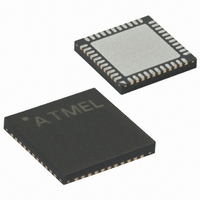
ATMEGA324P-A15MZ Atmel, ATMEGA324P-A15MZ Datasheet - Page 229

ATMEGA324P-A15MZ
Manufacturer Part Number
ATMEGA324P-A15MZ
Description
MCU AVR 32KB FLASH 15MHZ 44-VQFN
Manufacturer
Atmel
Series
AVR® ATmegar
Datasheet
1.ATMEGA324P-A15MZ.pdf
(346 pages)
Specifications of ATMEGA324P-A15MZ
Package / Case
44-VQFN Exposed Pad
Voltage - Supply (vcc/vdd)
2.7 V ~ 5.5 V
Operating Temperature
-40°C ~ 125°C
Speed
16MHz
Number Of I /o
32
Eeprom Size
1K x 8
Core Processor
AVR
Program Memory Type
FLASH
Ram Size
2K x 8
Program Memory Size
32KB (32K x 8)
Data Converters
A/D 8x10b
Oscillator Type
Internal
Peripherals
Brown-out Detect/Reset, POR, PWM, WDT
Connectivity
I²C, SPI, UART/USART
Core Size
8-Bit
Lead Free Status / RoHS Status
Lead free / RoHS Compliant
- Current page: 229 of 346
- Download datasheet (3Mb)
Boundary-scan
Chain
Scanning the Digital
Port Pins
2503N–AVR–06/08
The Boundary-scan chain has the capability of driving and observing the logic levels on the digi-
tal I/O pins, as well as the boundary between digital and analog logic for analog circuitry having
Off-chip connection.
Figure 116
cell consists of a standard Boundary-scan cell for the Pull-up Enable – PUExn – function, and a
bi-directional pin cell that combines the three signals Output Control – OCxn, Output Data –
ODxn, and Input Data – IDxn, into only a two-stage Shift Register. The port and pin indexes are
not used in the following description.
The Boundary-scan logic is not included in the figures in the datasheet.
ple digital Port Pin as described in the section
details from
When no alternate port function is present, the Input Data – ID – corresponds to the PINxn Reg-
ister value (but ID has no synchronizer), Output Data corresponds to the PORT Register, Output
Control corresponds to the Data Direction – DD Register, and the Pull-up Enable – PUExn – cor-
responds to logic expression PUD · DDxn · PORTxn.
Digital alternate port functions are connected outside the dotted box in
scan chain read the actual pin value. For Analog function, there is a direct connection from the
external pin to the analog circuit, and a scan chain is inserted on the interface between the digi-
tal logic and the analog circuitry.
Figure 116. Boundary-scan Cell for Bidirectional Port Pin with Pull-up Function.
Pullup Enable (PUE)
Output Control (OC)
Output Data (OD)
Input Data (ID)
shows the Boundary-scan Cell for a bi-directional port pin with pull-up function. The
Figure 116
From Last Cell
0
1
replaces the dashed box in
0
1
0
1
0
1
ShiftDR
ClockDR
D
D
D
FF2
FF1
FF0
To Next Cell
Q
Q
Q
UpdateDR
“I/O Ports” on page
Figure
D
G
D
G
D
G
LD2
LD1
LD0
Q
Q
Q
117.
0
1
0
1
0
1
EXTEST
ATmega32(L)
49. The Boundary-scan
Figure 117
Figure 117
Vcc
Port Pin (PXn)
shows a sim-
to make the
229
Related parts for ATMEGA324P-A15MZ
Image
Part Number
Description
Manufacturer
Datasheet
Request
R

Part Number:
Description:
Manufacturer:
Atmel Corporation
Datasheet:

Part Number:
Description:
Manufacturer:
Atmel Corporation
Datasheet:

Part Number:
Description:
IC MCU AVR 32K FLASH 44-TQFP
Manufacturer:
Atmel
Datasheet:

Part Number:
Description:
IC MCU AVR 32K FLASH 44-QFN
Manufacturer:
Atmel
Datasheet:

Part Number:
Description:
IC MCU AVR 32K FLASH 40-DIP
Manufacturer:
Atmel
Datasheet:

Part Number:
Description:
MCU AVR 32K FLASH 20MHZ 44-QFN
Manufacturer:
Atmel
Datasheet:

Part Number:
Description:
MCU AVR 32KB FLASH 20MHZ 44TQFP
Manufacturer:
Atmel
Datasheet:

Part Number:
Description:
MCU AVR 32KB FLASH 20MHZ 44QFN
Manufacturer:
Atmel
Datasheet:

Part Number:
Description:
MCU AVR 32KB FLASH 20MHZ 44TQFP
Manufacturer:
Atmel
Datasheet:

Part Number:
Description:
MCU AVR 32K FLASH 20MHZ 44-QFN
Manufacturer:
Atmel
Datasheet:

Part Number:
Description:
MCU AVR 32K FLASH 15MHZ 44-TQFP
Manufacturer:
Atmel
Datasheet:


