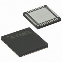
ATMEGA324P-A15MZ Atmel, ATMEGA324P-A15MZ Datasheet - Page 206

ATMEGA324P-A15MZ
Manufacturer Part Number
ATMEGA324P-A15MZ
Description
MCU AVR 32KB FLASH 15MHZ 44-VQFN
Manufacturer
Atmel
Series
AVR® ATmegar
Datasheet
1.ATMEGA324P-A15MZ.pdf
(346 pages)
Specifications of ATMEGA324P-A15MZ
Package / Case
44-VQFN Exposed Pad
Voltage - Supply (vcc/vdd)
2.7 V ~ 5.5 V
Operating Temperature
-40°C ~ 125°C
Speed
16MHz
Number Of I /o
32
Eeprom Size
1K x 8
Core Processor
AVR
Program Memory Type
FLASH
Ram Size
2K x 8
Program Memory Size
32KB (32K x 8)
Data Converters
A/D 8x10b
Oscillator Type
Internal
Peripherals
Brown-out Detect/Reset, POR, PWM, WDT
Connectivity
I²C, SPI, UART/USART
Core Size
8-Bit
Lead Free Status / RoHS Status
Lead free / RoHS Compliant
- Current page: 206 of 346
- Download datasheet (3Mb)
Differential Gain
Channels
206
ATmega32(L)
Figure 103. ADC Timing Diagram, Auto Triggered Conversion
Figure 104. ADC Timing Diagram, Free Running Conversion
Table 81. ADC Conversion Time
When using differential gain channels, certain aspects of the conversion need to be taken into
consideration.
Differential conversions are synchronized to the internal clock CK
clock. This synchronization is done automatically by the ADC interface in such a way that the
sample-and-hold occurs at a specific phase of CK
Condition
First conversion
Normal conversions, single ended
Auto Triggered conversions
Normal conversions, differential
Cycle Number
ADC Clock
Trigger
Source
ADATE
ADIF
ADCH
ADCL
Prescaler
Reset
Cycle Number
ADC Clock
ADSC
ADIF
ADCH
ADCL
MUX and REFS
Update
1
2
Conversion
Complete
3
One Conversion
Sample & Hold
11
4
Sample & Hold (Cycles
12
5
from Start of
Conversion)
6
1.5/2.5
13
13.5
1.5
2
7
One Conversion
Next Conversion
1
ADC2
MSB of Result
LSB of Result
8
. A conversion initiated by the user (i.e., all
2
MUX and REFS
Update
9
Conversion
10
3
Complete
Conversion Time (Cycles)
11
Sample & Hold
4
12
ADC2
13/14
13
13.5
25
13
equal to half the ADC
MSB of Result
LSB of Result
Next Conversion
2503N–AVR–06/08
1
Prescaler
Reset
2
Related parts for ATMEGA324P-A15MZ
Image
Part Number
Description
Manufacturer
Datasheet
Request
R

Part Number:
Description:
Manufacturer:
Atmel Corporation
Datasheet:

Part Number:
Description:
Manufacturer:
Atmel Corporation
Datasheet:

Part Number:
Description:
IC MCU AVR 32K FLASH 44-TQFP
Manufacturer:
Atmel
Datasheet:

Part Number:
Description:
IC MCU AVR 32K FLASH 44-QFN
Manufacturer:
Atmel
Datasheet:

Part Number:
Description:
IC MCU AVR 32K FLASH 40-DIP
Manufacturer:
Atmel
Datasheet:

Part Number:
Description:
MCU AVR 32K FLASH 20MHZ 44-QFN
Manufacturer:
Atmel
Datasheet:

Part Number:
Description:
MCU AVR 32KB FLASH 20MHZ 44TQFP
Manufacturer:
Atmel
Datasheet:

Part Number:
Description:
MCU AVR 32KB FLASH 20MHZ 44QFN
Manufacturer:
Atmel
Datasheet:

Part Number:
Description:
MCU AVR 32KB FLASH 20MHZ 44TQFP
Manufacturer:
Atmel
Datasheet:

Part Number:
Description:
MCU AVR 32K FLASH 20MHZ 44-QFN
Manufacturer:
Atmel
Datasheet:

Part Number:
Description:
MCU AVR 32K FLASH 15MHZ 44-TQFP
Manufacturer:
Atmel
Datasheet:


