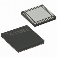
ATMEGA324P-A15MZ Atmel, ATMEGA324P-A15MZ Datasheet - Page 164

ATMEGA324P-A15MZ
Manufacturer Part Number
ATMEGA324P-A15MZ
Description
MCU AVR 32KB FLASH 15MHZ 44-VQFN
Manufacturer
Atmel
Series
AVR® ATmegar
Datasheet
1.ATMEGA324P-A15MZ.pdf
(346 pages)
Specifications of ATMEGA324P-A15MZ
Package / Case
44-VQFN Exposed Pad
Voltage - Supply (vcc/vdd)
2.7 V ~ 5.5 V
Operating Temperature
-40°C ~ 125°C
Speed
16MHz
Number Of I /o
32
Eeprom Size
1K x 8
Core Processor
AVR
Program Memory Type
FLASH
Ram Size
2K x 8
Program Memory Size
32KB (32K x 8)
Data Converters
A/D 8x10b
Oscillator Type
Internal
Peripherals
Brown-out Detect/Reset, POR, PWM, WDT
Connectivity
I²C, SPI, UART/USART
Core Size
8-Bit
Lead Free Status / RoHS Status
Lead free / RoHS Compliant
- Current page: 164 of 346
- Download datasheet (3Mb)
USART Baud Rate
Registers – UBRRL
and UBRRH
164
ATmega32(L)
• Bit 0 – UCPOL: Clock Polarity
This bit is used for Synchronous mode only. Write this bit to zero when Asynchronous mode is
used. The UCPOL bit sets the relationship between data output change and data input sample,
and the synchronous clock (XCK).
Table 67. UCPOL Bit Settings
The UBRRH Register shares the same I/O location as the UCSRC Register. See the
UBRRH/ UCSRC Registers” on page 158
• Bit 15 – URSEL: Register Select
This bit selects between accessing the UBRRH or the UCSRC Register. It is read as zero when
reading UBRRH. The URSEL must be zero when writing the UBRRH.
• Bit 14:12 – Reserved Bits
These bits are reserved for future use. For compatibility with future devices, these bit must be
written to zero when UBRRH is written.
• Bit 11:0 – UBRR11:0: USART Baud Rate Register
This is a 12-bit register which contains the USART baud rate. The UBRRH contains the four
most significant bits, and the UBRRL contains the 8 least significant bits of the USART baud
rate. Ongoing transmissions by the transmitter and receiver will be corrupted if the baud rate is
changed. Writing UBRRL will trigger an immediate update of the baud rate prescaler.
Bit
Read/Write
Initial Value
UCPOL
0
1
Transmitted Data Changed (Output of
TxD Pin)
Rising XCK Edge
Falling XCK Edge
URSEL
R/W
R/W
15
7
0
0
R/W
14
R
–
6
0
0
R/W
13
R
–
5
0
0
R/W
12
R
–
4
0
0
UBRR[7:0]
section which describes how to access this register.
R/W
R/W
11
3
0
0
Received Data Sampled (Input on
RxD Pin)
Falling XCK Edge
Rising XCK Edge
R/W
R/W
10
2
0
0
UBRR[11:8]
R/W
R/W
9
1
0
0
R/W
R/W
8
0
0
0
UBRRH
UBRRL
2503N–AVR–06/08
“Accessing
Related parts for ATMEGA324P-A15MZ
Image
Part Number
Description
Manufacturer
Datasheet
Request
R

Part Number:
Description:
Manufacturer:
Atmel Corporation
Datasheet:

Part Number:
Description:
Manufacturer:
Atmel Corporation
Datasheet:

Part Number:
Description:
IC MCU AVR 32K FLASH 44-TQFP
Manufacturer:
Atmel
Datasheet:

Part Number:
Description:
IC MCU AVR 32K FLASH 44-QFN
Manufacturer:
Atmel
Datasheet:

Part Number:
Description:
IC MCU AVR 32K FLASH 40-DIP
Manufacturer:
Atmel
Datasheet:

Part Number:
Description:
MCU AVR 32K FLASH 20MHZ 44-QFN
Manufacturer:
Atmel
Datasheet:

Part Number:
Description:
MCU AVR 32KB FLASH 20MHZ 44TQFP
Manufacturer:
Atmel
Datasheet:

Part Number:
Description:
MCU AVR 32KB FLASH 20MHZ 44QFN
Manufacturer:
Atmel
Datasheet:

Part Number:
Description:
MCU AVR 32KB FLASH 20MHZ 44TQFP
Manufacturer:
Atmel
Datasheet:

Part Number:
Description:
MCU AVR 32K FLASH 20MHZ 44-QFN
Manufacturer:
Atmel
Datasheet:

Part Number:
Description:
MCU AVR 32K FLASH 15MHZ 44-TQFP
Manufacturer:
Atmel
Datasheet:


