HD6417750SBP200 Renesas Electronics America, HD6417750SBP200 Datasheet - Page 12
HD6417750SBP200
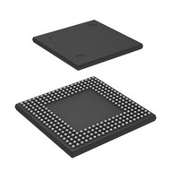
Manufacturer Part Number
HD6417750SBP200
Description
IC SUPERH MPU ROMLESS 256BGA
Manufacturer
Renesas Electronics America
Series
SuperH® SH7750r
Datasheet
1.D6417750RBP240DV.pdf
(1164 pages)
Specifications of HD6417750SBP200
Core Processor
SH-4
Core Size
32-Bit
Speed
200MHz
Connectivity
EBI/EMI, FIFO, SCI, SmartCard
Peripherals
DMA, POR, WDT
Number Of I /o
28
Program Memory Type
ROMless
Ram Size
24K x 8
Voltage - Supply (vcc/vdd)
1.8 V ~ 2.07 V
Oscillator Type
External
Operating Temperature
-20°C ~ 75°C
Package / Case
256-BGA
Lead Free Status / RoHS Status
Contains lead / RoHS non-compliant
Eeprom Size
-
Program Memory Size
-
Data Converters
-
Available stocks
Company
Part Number
Manufacturer
Quantity
Price

Part Number:
HD6417750SBP200
Manufacturer:
RENESAS/瑞萨
Quantity:
20 000


Rev.7.00 Oct. 10, 2008 Page x of lxxxiv
REJ09B0366-0700
Item
1.4.2 Pin Functions
(208-Pin QFP)
Table 1.3 Pin
Functions
1.4.3 Pin Functions
(264-Pin CSP)
Table 1.4 Pin
Functions
1.4.4 Pin Functions
(292-Pin BGA)
2.2.1 Privileged Mode
and Banks
Table 2.1 Initial
Register Values
2.6 Processor States
Figure 2.6 Processor
State Transitions
3.8 Usage Notes
4.3.1 Configuration
• LRU (SH7750R only)
Page
26, 27,
31
35, 38,
41
42 to 52 Newly added
55
68
109
119
Revision (See Manual for Details)
Table and notes amended
77
95
Notes: ... VSSQ, VSS, VSS-RTC, VSS-PLL1/2, and VSS-CPG
Table and notes amended
No.
90
91
92
93
113 T12
175 E14
Notes: ... Power must be supplied to VDD-RTC and VSS-RTC
Table amended
Type
Control registers
Figure amended
Newly added
Description amended
Pin
No.
From any state when
RESET = 0 and MRESET = 1
Pin
No.
U9
M9
P9
T9
CKIO
RD/WR
Pin Name
CKIO
VDDQ
CKIO2
RD/WR
RD/WR2
Pin Name
VSSQ
are connected inside the package.
The RD2, RD/WR2, CKIO2, and CKIO2ENB pins are not
provided on the QFP package.
regardless of whether or not the on-chip RTC is used.
NC pins must be left completely open, and not
connected to a power supply, GND, etc.
O
I/O
O
Registers
SR
O
O
I/O
O
Power IO VDD (3.3 V)
Power IO GND (0 V)
O
Power-on reset state
Function
Clock output
Read/write
Function
Clock output
CKIO*
Read/write
RD/WR
RESET = 0 and MRESET = 0
Reset
Reset
Initial Value*
MD bit = 1, RB bit = 1, BL bit = 1, FD bit = 0,
IMASK = 1111 (H'F), reserved bits = 0, others
undefined
RESET = 0,
MRESET = 1
CKIO
RD/WR RD/WR RD/WR RD/WR
SRAM
RD/WR RD/WR RD/WR RD/WR
RD/WR RD/WR RD/WR RD/WR
SRAM
CKIO
CKIO
DRAM
DRAM
Memory Interface
Memory Interface
CKIO
Manual reset state
SDRAM PCMCIA MPX
SDRAM PCMCIA MPX
CKIO
CKIO
Reset state
CKIO
RD/WR
CKIO
CKIO
RD/WR
RD/WR
Related parts for HD6417750SBP200
Image
Part Number
Description
Manufacturer
Datasheet
Request
R

Part Number:
Description:
KIT STARTER FOR M16C/29
Manufacturer:
Renesas Electronics America
Datasheet:

Part Number:
Description:
KIT STARTER FOR R8C/2D
Manufacturer:
Renesas Electronics America
Datasheet:

Part Number:
Description:
R0K33062P STARTER KIT
Manufacturer:
Renesas Electronics America
Datasheet:

Part Number:
Description:
KIT STARTER FOR R8C/23 E8A
Manufacturer:
Renesas Electronics America
Datasheet:

Part Number:
Description:
KIT STARTER FOR R8C/25
Manufacturer:
Renesas Electronics America
Datasheet:

Part Number:
Description:
KIT STARTER H8S2456 SHARPE DSPLY
Manufacturer:
Renesas Electronics America
Datasheet:

Part Number:
Description:
KIT STARTER FOR R8C38C
Manufacturer:
Renesas Electronics America
Datasheet:

Part Number:
Description:
KIT STARTER FOR R8C35C
Manufacturer:
Renesas Electronics America
Datasheet:

Part Number:
Description:
KIT STARTER FOR R8CL3AC+LCD APPS
Manufacturer:
Renesas Electronics America
Datasheet:
Part Number:
Description:
KIT STARTER FOR RX610
Manufacturer:
Renesas Electronics America
Datasheet:

Part Number:
Description:
KIT STARTER FOR R32C/118
Manufacturer:
Renesas Electronics America
Datasheet:

Part Number:
Description:
KIT DEV RSK-R8C/26-29
Manufacturer:
Renesas Electronics America
Datasheet:

Part Number:
Description:
KIT STARTER FOR SH7124
Manufacturer:
Renesas Electronics America
Datasheet:

Part Number:
Description:
KIT STARTER FOR H8SX/1622
Manufacturer:
Renesas Electronics America
Datasheet:

Part Number:
Description:
KIT DEV FOR SH7203
Manufacturer:
Renesas Electronics America
Datasheet: