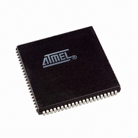
AT94K05AL-25AJI Atmel, AT94K05AL-25AJI Datasheet - Page 103

AT94K05AL-25AJI
Manufacturer Part Number
AT94K05AL-25AJI
Description
IC FPSLIC 5K GATE 25MHZ 84PLCC
Manufacturer
Atmel
Series
FPSLIC®r
Specifications of AT94K05AL-25AJI
Core Type
8-bit AVR
Speed
25MHz
Interface
I²C, UART
Program Sram Bytes
4K-16K
Fpga Sram
2kb
Data Sram Bytes
4K ~ 16K
Fpga Core Cells
256
Fpga Gates
5K
Fpga Registers
436
Voltage - Supply
3 V ~ 3.6 V
Mounting Type
Surface Mount
Operating Temperature
-40°C ~ 85°C
Package / Case
84-PLCC
For Use With
ATSTK594 - BOARD FPSLIC DAUGHTER FOR STK500
Lead Free Status / RoHS Status
Contains lead / RoHS non-compliant
Eeprom Size
-
Available stocks
Company
Part Number
Manufacturer
Quantity
Price
- Current page: 103 of 204
- Download datasheet (4Mb)
1138I–FPSLI–1/08
Table 4-17.
Notes:
• Bit 3 - FOC1A: Force Output Compare1A
Writing a logic 1 to this bit forces a change in the compare match output pin PE6 according to
the values already set in COM1A1 and COM1A0. If the COM1A1 and COM1A0 bits are written
in the same cycle as FOC1A, the new settings will not take effect until next compare match or
forced compare match occurs. The Force Output Compare bit can be used to change the output
pin without waiting for a compare match in the timer. The automatic action programmed in
COM1A1 and COM1A0 happens as if a Compare Match had occurred, but no interrupt is gener-
ated and it will not clear the timer even if CTC1 in TCCR1B is set. The FOC1A bit will always be
read as zero. The setting of the FOC1A bit has no effect in PWM mode.
• Bit 2 - FOC1B: Force Output Compare1B
Writing a logic 1 to this bit forces a change in the compare match output pin PE5 according to
the values already set in COM1B1 and COM1B0. If the COM1B1 and COM1B0 bits are written
in the same cycle as FOC1B, the new settings will not take effect until next compare match or
forced compare match occurs. The Force Output Compare bit can be used to change the output
pin without waiting for a compare match in the timer. The automatic action programmed in
COM1B1 and COM1B0 happens as if a Compare Match had occurred, but no interrupt is gener-
ated. The FOC1B bit will always be read as zero. The setting of the FOC1B bit has no effect in
PWM mode.
• Bits 1..0 - PWM11, PWM10: Pulse Width Modulator Select Bits
These bits select PWM operation of Timer/Counter1 as specified in
described on
Table 4-18.
COM1X1
PWM11
0
0
1
1
0
0
1
1
1. In PWM mode, these bits have a different function. Refer to
2. X = A or B
(2)
description.
page
Compare 1 Mode Select
PWM Mode Select
COM1X0
PWM10
107.
0
1
0
1
0
1
0
1
(2)
Description
Timer/Counter1 disconnected from output pin OC1X
Toggles the OC1X output line
Clears the OC1X output line (to zero)
Sets the OC1X output line (to one)
Description
PWM operation of Timer/Counter1 is disabled
Timer/Counter1 is an 8-bit PWM
Timer/Counter1 is a 9-bit PWM
Timer/Counter1 is a 10-bit PWM
(1)
AT94KAL Series FPSLIC
Table 4-21
Table
for a detailed
4-18. This mode is
103
Related parts for AT94K05AL-25AJI
Image
Part Number
Description
Manufacturer
Datasheet
Request
R

Part Number:
Description:
IC FPSLIC 5K GATE 25MHZ 84PLCC
Manufacturer:
Atmel
Datasheet:

Part Number:
Description:
Fpslic Devices Combine 5K Gates of Atmel's Patented AT40K Fpga Architecture, a 20 Mips Avr 8-bit Risc Microprocessor Core, Numerous Fixed Microcontroller Peripheries And up to 36K Bytes of Program And Data SRAM.
Manufacturer:
ATMEL Corporation
Datasheet:

Part Number:
Description:
IC FPSLIC 5K GATE 25MHZ 208PQFP
Manufacturer:
Atmel
Datasheet:

Part Number:
Description:
IC FPSLIC 5K GATE 25MHZ 144LQFP
Manufacturer:
Atmel
Datasheet:

Part Number:
Description:
IC FPSLIC 5K GATE 25MHZ 208PQFP
Manufacturer:
Atmel
Datasheet:

Part Number:
Description:
IC FPSLIC 5K GATE 25MHZ 144LQFP
Manufacturer:
Atmel
Datasheet:

Part Number:
Description:
IC FPSLIC 5K GATE 25MHZ 144-LQFP
Manufacturer:
Atmel
Datasheet:

Part Number:
Description:
IC FPSLIC 5K GATE 25MHZ 100-TQFP
Manufacturer:
Atmel
Datasheet:

Part Number:
Description:
Manufacturer:
Atmel
Datasheet:

Part Number:
Description:
Manufacturer:
Atmel
Datasheet:

Part Number:
Description:
Manufacturer:
Atmel
Datasheet:

Part Number:
Description:
5k - 40k Gates Of At40k Fpga With 8-bit Microcontroller, Up To 36k Bytes Of Sram And On-chip Jtag Ice
Manufacturer:
ATMEL Corporation
Datasheet:

Part Number:
Description:
At94k05al 5k - 40k Gates Of At40k Fpga With 8-bit Microcontroller, Up To 36k Bytes Of Sram And On-chip Jtag Ice
Manufacturer:
ATMEL Corporation
Datasheet:

Part Number:
Description:
DEV KIT FOR AVR/AVR32
Manufacturer:
Atmel
Datasheet:


