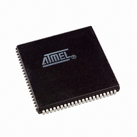
AT94K05AL-25AJI Atmel, AT94K05AL-25AJI Datasheet - Page 80

AT94K05AL-25AJI
Manufacturer Part Number
AT94K05AL-25AJI
Description
IC FPSLIC 5K GATE 25MHZ 84PLCC
Manufacturer
Atmel
Series
FPSLIC®r
Specifications of AT94K05AL-25AJI
Core Type
8-bit AVR
Speed
25MHz
Interface
I²C, UART
Program Sram Bytes
4K-16K
Fpga Sram
2kb
Data Sram Bytes
4K ~ 16K
Fpga Core Cells
256
Fpga Gates
5K
Fpga Registers
436
Voltage - Supply
3 V ~ 3.6 V
Mounting Type
Surface Mount
Operating Temperature
-40°C ~ 85°C
Package / Case
84-PLCC
For Use With
ATSTK594 - BOARD FPSLIC DAUGHTER FOR STK500
Lead Free Status / RoHS Status
Contains lead / RoHS non-compliant
Eeprom Size
-
Available stocks
Company
Part Number
Manufacturer
Quantity
Price
- Current page: 80 of 204
- Download datasheet (4Mb)
4.22.2.2
4.22.2.3
4.22.2.4
4.22.2.5
4.22.3
4.22.3.1
80
AT94KAL Series FPSLIC
Boundary-scan Chain
IDCODE; $1
SAMPLE_PRELOAD; $2
AVR_RESET; $C
BYPASS; $F
Scanning the Digital Port Pins
Optional JTAG instruction selecting the 32-bit ID register as Data Register. The ID register con-
sists of a version number, a device number and the manufacturer code chosen by JEDEC. This
is the default instruction after power-up.
The active states are:
Mandatory JTAG instruction for pre-loading the output latches and taking a snap-shot of the
input/output pins without affecting the system operation. However, the output latches are not
connected to the pins. The Boundary-Scan Chain is selected as Data Register.
The active states are:
The AVR specific public JTAG instruction for forcing the AVR device into the Reset Mode or
releasing the JTAG reset source. The TAP controller is not reset by this instruction. The one bit
Reset Register is selected as Data Register. Note that the reset will be active as long as there is
a logic “1” in the Reset Chain. The output from this chain is not latched.
The active state is:
Mandatory JTAG instruction selecting the Bypass Register for Data Register.
The active states are:
The Boundary-Scan chain has the capability of driving and observing the logic levels on the
AVR’s digital I/O pins.
Figure 4-20
cell consists of a standard boundary-scan cell for the pull-up function, and a bi-directional pin
cell that combines the three signals Output Control (OC), Output Data (OD), and Input Data (ID),
into only a two-stage shift register.
• Capture-DR: Data on the external pins are sampled into the Boundary-Scan Chain.
• Shift-DR: The Internal Scan Chain is shifted by the TCK input.
• Update-DR: Data from the scan chain is applied to output pins.
• Capture-DR: Data in the IDCODE register is sampled into the Boundary-Scan Chain.
• Shift-DR: The IDCODE scan chain is shifted by the TCK input.
• Capture-DR: Data on the external pins are sampled into the Boundary-Scan Chain.
• Shift-DR: The Boundary-Scan Chain is shifted by the TCK input.
• Update-DR: Data from the Boundary-Scan chain is applied to the output latches. However,
• Shift-DR: The Reset Register is shifted by the TCK input.
• Capture-DR: Loads a logic “0” into the Bypass Register.
• Shift-DR: The Bypass Register cell between TDI and TDO is shifted.
the output latches are not connected to the pins.
shows the boundary-scan cell for bi-directional port pins with pull-up function. The
1138I–FPSLI–1/08
Related parts for AT94K05AL-25AJI
Image
Part Number
Description
Manufacturer
Datasheet
Request
R

Part Number:
Description:
IC FPSLIC 5K GATE 25MHZ 84PLCC
Manufacturer:
Atmel
Datasheet:

Part Number:
Description:
Fpslic Devices Combine 5K Gates of Atmel's Patented AT40K Fpga Architecture, a 20 Mips Avr 8-bit Risc Microprocessor Core, Numerous Fixed Microcontroller Peripheries And up to 36K Bytes of Program And Data SRAM.
Manufacturer:
ATMEL Corporation
Datasheet:

Part Number:
Description:
IC FPSLIC 5K GATE 25MHZ 208PQFP
Manufacturer:
Atmel
Datasheet:

Part Number:
Description:
IC FPSLIC 5K GATE 25MHZ 144LQFP
Manufacturer:
Atmel
Datasheet:

Part Number:
Description:
IC FPSLIC 5K GATE 25MHZ 208PQFP
Manufacturer:
Atmel
Datasheet:

Part Number:
Description:
IC FPSLIC 5K GATE 25MHZ 144LQFP
Manufacturer:
Atmel
Datasheet:

Part Number:
Description:
IC FPSLIC 5K GATE 25MHZ 144-LQFP
Manufacturer:
Atmel
Datasheet:

Part Number:
Description:
IC FPSLIC 5K GATE 25MHZ 100-TQFP
Manufacturer:
Atmel
Datasheet:

Part Number:
Description:
Manufacturer:
Atmel
Datasheet:

Part Number:
Description:
Manufacturer:
Atmel
Datasheet:

Part Number:
Description:
Manufacturer:
Atmel
Datasheet:

Part Number:
Description:
5k - 40k Gates Of At40k Fpga With 8-bit Microcontroller, Up To 36k Bytes Of Sram And On-chip Jtag Ice
Manufacturer:
ATMEL Corporation
Datasheet:

Part Number:
Description:
At94k05al 5k - 40k Gates Of At40k Fpga With 8-bit Microcontroller, Up To 36k Bytes Of Sram And On-chip Jtag Ice
Manufacturer:
ATMEL Corporation
Datasheet:

Part Number:
Description:
DEV KIT FOR AVR/AVR32
Manufacturer:
Atmel
Datasheet:


