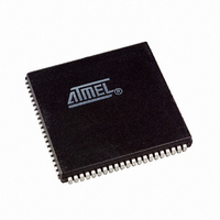
AT94K05AL-25AJI Atmel, AT94K05AL-25AJI Datasheet - Page 59

AT94K05AL-25AJI
Manufacturer Part Number
AT94K05AL-25AJI
Description
IC FPSLIC 5K GATE 25MHZ 84PLCC
Manufacturer
Atmel
Series
FPSLIC®r
Specifications of AT94K05AL-25AJI
Core Type
8-bit AVR
Speed
25MHz
Interface
I²C, UART
Program Sram Bytes
4K-16K
Fpga Sram
2kb
Data Sram Bytes
4K ~ 16K
Fpga Core Cells
256
Fpga Gates
5K
Fpga Registers
436
Voltage - Supply
3 V ~ 3.6 V
Mounting Type
Surface Mount
Operating Temperature
-40°C ~ 85°C
Package / Case
84-PLCC
For Use With
ATSTK594 - BOARD FPSLIC DAUGHTER FOR STK500
Lead Free Status / RoHS Status
Contains lead / RoHS non-compliant
Eeprom Size
-
Available stocks
Company
Part Number
Manufacturer
Quantity
Price
- Current page: 59 of 204
- Download datasheet (4Mb)
4.15
1138I–FPSLI–1/08
FPGA I/O Interrupt Control by AVR
This is an alternate memory space for the FPGA I/O Select addresses. If the FIADR bit in the
FISCR register is set to logic 1, the four I/O addresses, FISUA - FISUD, are mapped to physical
registers and provide memory space for FPGA interrupt masking and interrupt flag status. If the
FIADR bit in the FISCR register is cleared to a logic 0, the I/O register addresses will be
decoded into FPGA select lines.
All FPGA interrupt lines into the AVR are negative edge triggered. See
priority.
Interrupt Control Registers – FISUA..D
• Bits 7..4 - FIF3 - 0: FPGA Interrupt Flags 3 - 0
The 16 FPGA interrupt flag bits all work the same. Each is set (one) by a valid negative edge
transition on its associated interrupt line from the FPGA. Valid transitions are defined as any
change in state preceded by at least two cycles of the old state and succeeded by at least two
cycles of the new state. Therefore, it is required that interrupt lines transition from 1 to 0 at
least two cycles after the line is stable High; the line must then remain stable Low for at
least two cycles following the transition. Each bit is cleared by the hardware when executing
the corresponding interrupt handling vector. Alternatively, each bit will be cleared by writing a
logic 1 to it. When the I-bit in the Status Register, the corresponding FPGA interrupt mask bit
and the given FPGA interrupt flag bit are set (one), the associated interrupt is executed.
• Bits 7..4 - FIF7 - 4: FPGA Interrupt Flags 7 - 4
See Bits 7..4 - FIF3 - 0: FPGA Interrupt Flags 3 - 0.
• Bits 7..4 - FIF11 - 8: FPGA Interrupt Flags 11 - 8
See Bits 7..4 - FIF3 - 0: FPGA Interrupt Flags 3 - 0. Not available on the AT94K05.
• Bits 7..4 - FIF15 - 12: FPGA Interrupt Flags 15 - 12
See Bits 7..4 - FIF3 - 0: FPGA Interrupt Flags 3 - 0. Not available on the AT94K05.
• Bits 3..0 - FINT3 - 0: FPGA Interrupt Masks 3 - 0
The 16 FPGA interrupt mask bits all work the same. When a mask bit is set (one) and the I-bit in
the Status Register is set (one), the given FPGA interrupt is enabled. The corresponding inter-
rupt handling vector is executed when the given FPGA interrupt flag bit is set (one) by a negative
edge transition on the associated interrupt line from the FPGA.
Note:
• Bits 3..0 - FINT7 - 4: FPGA Interrupt Masks 7 - 4
See Bits 3..0 - FINT3 - 0: FPGA Interrupt Masks 3 - 0.
Bit
$14 ($34)
$15 ($35)
$16 ($36)
$17 ($37)
Read/Write
Initial Value
1. FPGA interrupts 3 - 0 will cause a wake-up from the AVR Sleep modes. These interrupts are
treated as low-level triggered in the Power-down and Power-save modes, see
on page
7
FIF3
FIF7
FIF11
FIF15
R/W
0
69.
6
FIF2
FIF6
FIF10
FIF14
R/W
0
5
FIF1
FIF5
FIF9
FIF13
R/W
0
4
FIF0
FIF4
FIF8
FIF12
R/W
0
AT94KAL Series FPSLIC
3
FINT3
FINT7
FINT11
FINT15
R/W
0
(1)
2
FINT2
FINT6
FINT10
FINT14
R/W
0
1
FINT1
FINT5
FINT9
FINT13
R/W
0
page 60
0
FINT0
FINT4
FINT8
FINT12
R/W
0
“Sleep Modes”
for interrupt
FISUA
FSUB
FISUC
FISUD
59
Related parts for AT94K05AL-25AJI
Image
Part Number
Description
Manufacturer
Datasheet
Request
R

Part Number:
Description:
IC FPSLIC 5K GATE 25MHZ 84PLCC
Manufacturer:
Atmel
Datasheet:

Part Number:
Description:
Fpslic Devices Combine 5K Gates of Atmel's Patented AT40K Fpga Architecture, a 20 Mips Avr 8-bit Risc Microprocessor Core, Numerous Fixed Microcontroller Peripheries And up to 36K Bytes of Program And Data SRAM.
Manufacturer:
ATMEL Corporation
Datasheet:

Part Number:
Description:
IC FPSLIC 5K GATE 25MHZ 208PQFP
Manufacturer:
Atmel
Datasheet:

Part Number:
Description:
IC FPSLIC 5K GATE 25MHZ 144LQFP
Manufacturer:
Atmel
Datasheet:

Part Number:
Description:
IC FPSLIC 5K GATE 25MHZ 208PQFP
Manufacturer:
Atmel
Datasheet:

Part Number:
Description:
IC FPSLIC 5K GATE 25MHZ 144LQFP
Manufacturer:
Atmel
Datasheet:

Part Number:
Description:
IC FPSLIC 5K GATE 25MHZ 144-LQFP
Manufacturer:
Atmel
Datasheet:

Part Number:
Description:
IC FPSLIC 5K GATE 25MHZ 100-TQFP
Manufacturer:
Atmel
Datasheet:

Part Number:
Description:
Manufacturer:
Atmel
Datasheet:

Part Number:
Description:
Manufacturer:
Atmel
Datasheet:

Part Number:
Description:
Manufacturer:
Atmel
Datasheet:

Part Number:
Description:
5k - 40k Gates Of At40k Fpga With 8-bit Microcontroller, Up To 36k Bytes Of Sram And On-chip Jtag Ice
Manufacturer:
ATMEL Corporation
Datasheet:

Part Number:
Description:
At94k05al 5k - 40k Gates Of At40k Fpga With 8-bit Microcontroller, Up To 36k Bytes Of Sram And On-chip Jtag Ice
Manufacturer:
ATMEL Corporation
Datasheet:

Part Number:
Description:
DEV KIT FOR AVR/AVR32
Manufacturer:
Atmel
Datasheet:


