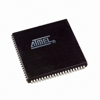
AT94K05AL-25AJI Atmel, AT94K05AL-25AJI Datasheet - Page 49

AT94K05AL-25AJI
Manufacturer Part Number
AT94K05AL-25AJI
Description
IC FPSLIC 5K GATE 25MHZ 84PLCC
Manufacturer
Atmel
Series
FPSLIC®r
Specifications of AT94K05AL-25AJI
Core Type
8-bit AVR
Speed
25MHz
Interface
I²C, UART
Program Sram Bytes
4K-16K
Fpga Sram
2kb
Data Sram Bytes
4K ~ 16K
Fpga Core Cells
256
Fpga Gates
5K
Fpga Registers
436
Voltage - Supply
3 V ~ 3.6 V
Mounting Type
Surface Mount
Operating Temperature
-40°C ~ 85°C
Package / Case
84-PLCC
For Use With
ATSTK594 - BOARD FPSLIC DAUGHTER FOR STK500
Lead Free Status / RoHS Status
Contains lead / RoHS non-compliant
Eeprom Size
-
Available stocks
Company
Part Number
Manufacturer
Quantity
Price
- Current page: 49 of 204
- Download datasheet (4Mb)
4.11.1
Note:
1138I–FPSLI–1/08
$0E ($2E)
$0D ($2D)
$0C ($2C)
$0B ($2B)
$0A ($2A)
$16 ($36)
$15 ($35)
$14 ($34)
$13 ($33)
$12 ($32)
$11 ($31)
$10 ($30)
$0F ($2F)
$09 ($29)
$08 ($28)
$07 ($27)
$06 ($26)
$05 ($25)
$04 ($24)
$03 ($23)
$02 ($22)
$01 ($21)
$00 ($20)
Address
1. The On-chip Debug Register (OCDR) is detailed on the “FPSLIC On-chip Debug System” distributed within Atmel and select
AT94K Register Summary (Continued)
third-party vendors only under Non-Disclosure Agreement (NDA). Contact fpslic@atmel.com for a copy of this document.
Name
FISUC
FISUB
FISUA
FISCR
PORTD
DDRD
PIND
Reserved
Reserved
Reserved
UDR0
UCSR0A
UCSR0B
UBRR0
OCDR
(Reserved)
PORTE
DDRE
PINE
Reserved
UDR1
UCSR1A
UCSR1B
UBRR1
FPGA I/O Select, Interrupt Mask/Flag Register C (Reserved on AT94K05)
FPGA I/O Select, Interrupt Mask/Flag Register B
FPGA I/O Select, Interrupt Mask/Flag Register A
UART0 I/O Data Register
UART0 Baud-rate Register
UART1 I/O Data Register
UART1 Baud-rate Register
PORTD7
PORTE7
RXCIE0
RXCIE1
DDRD7
DDRE7
The embedded AVR core I/Os and peripherals, and all the virtual FPGA peripherals are placed
in the I/O space. The different I/O locations are directly accessed by the IN and OUT instructions
transferring data between the 32 x 8 general-purpose working registers and the I/O space. I/O
registers within the address range $00 – $1F are directly bit-accessible using the SBI and CBI
instructions. In these registers, the value of single bits can be checked by using the SBIS and
SBIC instructions. When using the I/O specific instructions IN, OUT, the I/O register address
$00 – $3F are used, see
added to this address. All I/O register addresses throughout this document are shown with the
SRAM address in parentheses.
FIADR
PIND7
PINE7
RXC0
RXC1
IDRD
Bit 7
PORTD6
PORTE6
TXCIE0
TXCIE1
DDRD6
DDRE6
PIND6
PINE6
TXC0
TXC1
Bit 6
PORTD5
PORTE5
UDRIE0
UDRIE1
DDRD5
UDRE0
DDRE5
UDRE1
PIND5
PINE5
Bit 5
Figure
PORTD4
PORTE4
DDRD4
RXEN0
DDRE4
RXEN1
PIND4
PINE4
Bit 4
FE0
FE1
4-9. When addressing I/O registers as SRAM, $20 must be
PORTD3
PORTE3
DDRD3
DDRE3
TXEN0
TXEN1
PIND3
PINE3
Bit 3
OR0
OR1
AT94KAL Series FPSLIC
PORTD2
PORTE2
DDRD2
DDRE2
CHR90
CHR91
PIND2
PINE2
Bit 2
PORTD1
PORTE1
DDRD1
DDRE1
RXB80
RXB81
PIND1
PINE1
XFIS1
U2X0
U2X1
Bit 1
PORTD0
PORTE0
MPCM0
MPCM1
DDRD0
DDRE0
TXB80
TXB81
PIND0
PINE0
XFIS0
Bit 0
Reserved
Reference
54, 56
54, 56
54, 56
Page
124
124
124
101
101
103
105
126
126
126
101
101
103
105
53
(1)
49
Related parts for AT94K05AL-25AJI
Image
Part Number
Description
Manufacturer
Datasheet
Request
R

Part Number:
Description:
IC FPSLIC 5K GATE 25MHZ 84PLCC
Manufacturer:
Atmel
Datasheet:

Part Number:
Description:
Fpslic Devices Combine 5K Gates of Atmel's Patented AT40K Fpga Architecture, a 20 Mips Avr 8-bit Risc Microprocessor Core, Numerous Fixed Microcontroller Peripheries And up to 36K Bytes of Program And Data SRAM.
Manufacturer:
ATMEL Corporation
Datasheet:

Part Number:
Description:
IC FPSLIC 5K GATE 25MHZ 208PQFP
Manufacturer:
Atmel
Datasheet:

Part Number:
Description:
IC FPSLIC 5K GATE 25MHZ 144LQFP
Manufacturer:
Atmel
Datasheet:

Part Number:
Description:
IC FPSLIC 5K GATE 25MHZ 208PQFP
Manufacturer:
Atmel
Datasheet:

Part Number:
Description:
IC FPSLIC 5K GATE 25MHZ 144LQFP
Manufacturer:
Atmel
Datasheet:

Part Number:
Description:
IC FPSLIC 5K GATE 25MHZ 144-LQFP
Manufacturer:
Atmel
Datasheet:

Part Number:
Description:
IC FPSLIC 5K GATE 25MHZ 100-TQFP
Manufacturer:
Atmel
Datasheet:

Part Number:
Description:
Manufacturer:
Atmel
Datasheet:

Part Number:
Description:
Manufacturer:
Atmel
Datasheet:

Part Number:
Description:
Manufacturer:
Atmel
Datasheet:

Part Number:
Description:
5k - 40k Gates Of At40k Fpga With 8-bit Microcontroller, Up To 36k Bytes Of Sram And On-chip Jtag Ice
Manufacturer:
ATMEL Corporation
Datasheet:

Part Number:
Description:
At94k05al 5k - 40k Gates Of At40k Fpga With 8-bit Microcontroller, Up To 36k Bytes Of Sram And On-chip Jtag Ice
Manufacturer:
ATMEL Corporation
Datasheet:

Part Number:
Description:
DEV KIT FOR AVR/AVR32
Manufacturer:
Atmel
Datasheet:


