AT94K05AL-25AJI Atmel, AT94K05AL-25AJI Datasheet - Page 99
AT94K05AL-25AJI
Manufacturer Part Number
AT94K05AL-25AJI
Description
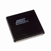
IC FPSLIC 5K GATE 25MHZ 84PLCC
Manufacturer
Atmel
Series
FPSLIC®r
Specifications of AT94K05AL-25AJI
Core Type
8-bit AVR
Speed
25MHz
Interface
I²C, UART
Program Sram Bytes
4K-16K
Fpga Sram
2kb
Data Sram Bytes
4K ~ 16K
Fpga Core Cells
256
Fpga Gates
5K
Fpga Registers
436
Voltage - Supply
3 V ~ 3.6 V
Mounting Type
Surface Mount
Operating Temperature
-40°C ~ 85°C
Package / Case
84-PLCC
For Use With
ATSTK594 - BOARD FPSLIC DAUGHTER FOR STK500
Lead Free Status / RoHS Status
Contains lead / RoHS non-compliant
Eeprom Size
-
Available stocks
Company
Part Number
Manufacturer
Quantity
Price


4.25.3
1138I–FPSLI–1/08
Asynchronous Operation of Timer/Counter2
If a write is performed to any of the three Timer/Counter2 registers while its update busy flag is
set (one), the updated value might get corrupted and cause an unintentional interrupt to occur.
The mechanisms for reading TCNT2, OCR2 and TCCR2 are different. When reading TCNT2,
the actual timer value is read. When reading OCR2 or TCCR2, the value in the temporary stor-
age register is read.
When Timer/Counter2 operates asynchronously, some considerations must be taken:
• When switching between asynchronous and synchronous clocking of Timer/Counter2, the
• The oscillator is optimized for use with a 32.768 kHz watch crystal. An external clock signal
• When writing to one of the registers TCNT2, OCR2, or TCCR2, the value is transferred to a
• When entering Power-save mode after having written to TCNT2, OCR2, or TCCR2, the user
• If Timer/Counter2 is used to wake-up the device from Power-save mode, precautions must be
• When asynchronous operation is selected, the 32.768 kHz oscillator for Timer/Counter2 is
timer registers TCNT2, OCR2 and TCCR2 might get corrupted. A safe procedure for
switching the clock source is:
applied to this pin goes through the same amplifier having a bandwidth of 256 kHz. The
external clock signal should therefore be in the interval
0 Hz – 1 MHz. The frequency of the clock signal applied to the TOSC1 pin must be lower
than one fourth of the CPU main clock frequency.
temporary register, and latched after two positive edges on TOSC1. The user should not
write a new value before the contents of the temporary register have been transferred to its
destination. Each of the three mentioned registers have their individual temporary register,
which means that, e.g., writing to TCNT2 does not disturb an OCR2 write in progress. To
detect that a transfer to the destination register has taken place, an Asynchronous Status
Register – ASSR has been implemented.
must wait until the written register has been updated if Timer/Counter2 is used to wake-up
the device. Otherwise, the MCU will go to sleep before the changes have had any effect. This
is extremely important if the Output Compare2 interrupt is used to wake-up the device;
Output compare is disabled during write to OCR2 or TCNT2. If the write cycle is not finished
(i.e., the MCU enters Sleep mode before the OCR2UB bit returns to zero), the device will
never get a compare match and the MCU will not wake-up.
taken if the user wants to re-enter Power-save mode: The interrupt logic needs one TOSC1
cycle to be reset. If the time between wake-up and reentering Power-save mode is less than
one TOSC1 cycle, the interrupt will not occur and the device will fail to wake up. If the user is
in doubt whether the time before re-entering power-save is sufficient, the following algorithm
can be used to ensure that one TOSC1 cycle has elapsed:
always running, except in Power-down mode. After a power-up reset or wake-up from power-
1. Disable the Timer/Counter2 interrupts by clearing OCIE2 and TOIE2.
2. Select clock source by setting AS2 as appropriate.
3. Write new values to TCNT2, OCR2 and TCCR2.
4. To switch to asynchronous operation: Wait for TCN2UB, OCR2UB, and TCR2UB.
5. Enable interrupts, if needed.
1. Write a value to TCCR2, TCNT2, or OCR2.
2. Wait until the corresponding Update Busy flag in ASSR returns to zero.
3. Enter Power-save mode.
AT94KAL Series FPSLIC
99
Related parts for AT94K05AL-25AJI
Image
Part Number
Description
Manufacturer
Datasheet
Request
R

Part Number:
Description:
IC FPSLIC 5K GATE 25MHZ 84PLCC
Manufacturer:
Atmel
Datasheet:

Part Number:
Description:
Fpslic Devices Combine 5K Gates of Atmel's Patented AT40K Fpga Architecture, a 20 Mips Avr 8-bit Risc Microprocessor Core, Numerous Fixed Microcontroller Peripheries And up to 36K Bytes of Program And Data SRAM.
Manufacturer:
ATMEL Corporation
Datasheet:

Part Number:
Description:
IC FPSLIC 5K GATE 25MHZ 208PQFP
Manufacturer:
Atmel
Datasheet:

Part Number:
Description:
IC FPSLIC 5K GATE 25MHZ 144LQFP
Manufacturer:
Atmel
Datasheet:
Part Number:
Description:
IC FPSLIC 5K GATE 25MHZ 208PQFP
Manufacturer:
Atmel
Datasheet:
Part Number:
Description:
IC FPSLIC 5K GATE 25MHZ 144LQFP
Manufacturer:
Atmel
Datasheet:

Part Number:
Description:
IC FPSLIC 5K GATE 25MHZ 144-LQFP
Manufacturer:
Atmel
Datasheet:

Part Number:
Description:
IC FPSLIC 5K GATE 25MHZ 100-TQFP
Manufacturer:
Atmel
Datasheet:
Part Number:
Description:
Manufacturer:
Atmel
Datasheet:
Part Number:
Description:
Manufacturer:
Atmel
Datasheet:
Part Number:
Description:
Manufacturer:
Atmel
Datasheet:
Part Number:
Description:
5k - 40k Gates Of At40k Fpga With 8-bit Microcontroller, Up To 36k Bytes Of Sram And On-chip Jtag Ice
Manufacturer:
ATMEL Corporation
Datasheet:
Part Number:
Description:
At94k05al 5k - 40k Gates Of At40k Fpga With 8-bit Microcontroller, Up To 36k Bytes Of Sram And On-chip Jtag Ice
Manufacturer:
ATMEL Corporation
Datasheet:

Part Number:
Description:
DEV KIT FOR AVR/AVR32
Manufacturer:
Atmel
Datasheet: