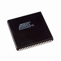
AT94K05AL-25AJI Atmel, AT94K05AL-25AJI Datasheet - Page 85

AT94K05AL-25AJI
Manufacturer Part Number
AT94K05AL-25AJI
Description
IC FPSLIC 5K GATE 25MHZ 84PLCC
Manufacturer
Atmel
Series
FPSLIC®r
Specifications of AT94K05AL-25AJI
Core Type
8-bit AVR
Speed
25MHz
Interface
I²C, UART
Program Sram Bytes
4K-16K
Fpga Sram
2kb
Data Sram Bytes
4K ~ 16K
Fpga Core Cells
256
Fpga Gates
5K
Fpga Registers
436
Voltage - Supply
3 V ~ 3.6 V
Mounting Type
Surface Mount
Operating Temperature
-40°C ~ 85°C
Package / Case
84-PLCC
For Use With
ATSTK594 - BOARD FPSLIC DAUGHTER FOR STK500
Lead Free Status / RoHS Status
Contains lead / RoHS non-compliant
Eeprom Size
-
Available stocks
Company
Part Number
Manufacturer
Quantity
Price
- Current page: 85 of 204
- Download datasheet (4Mb)
4.22.4
1138I–FPSLI–1/08
FPSLIC Boundary-scan Order
Scanning an oscillator output gives unpredictable results as there is a frequency drift between
the internal oscillator and the JTAG TCK clock.
The clock configuration is programmed in the SCR. As an SCR bit is not changed run-time, the
clock configuration is considered fixed for a given application. The user is advised to scan the
same clock option as to be used in the final system. The enable signals are supported in the
scan chain because the system logic can disable clock options in sleep modes, thereby discon-
necting the oscillator pins from the scan path if not provided.
The XTAL or TOSC “Clock In” Scan chain bit will always capture “1” if the oscillator is disabled
(“Enable Clock” bit is active Low).
Table 4-11
selected as data path. Bit 0 is the LSB; the first bit scanned in, and the first bit scanned out. In
Figure
FF1, and “Pull-up – PXn” corresponds to FF2.
Table 4-11.
4-20, “Data Out/In – PXn” corresponds to FF0, “Enable Output – PXn” corresponds to
I/O Ports
PORTE
shows the Scan order between TDI and TDO when the Boundary-Scan chain is
AVR I/O Boundary Scan – JTAG Instructions $0/$2
AT94KAL Series FPSLIC
Enable Output - PE7
Enable Output - PE6
Enable Output - PE5
Enable Output - PE4
Enable Output - PE3
Enable Output - PE2
Enable Output - PE1
Enable Output - PE0
Data Out/In - PE7
Data Out/In - PE6
Data Out/In - PE5
Data Out/In - PE4
Data Out/In - PE3
Data Out/In - PE2
Data Out/In - PE1
Data Out/In - PE0
Pull-up - PE7
Pull-up - PE6
Pull-up - PE5
Pull-up - PE4
Pull-up - PE3
Pull-up - PE2
Pull-up - PE1
Pull-up - PE0
Description
Bit
68
67
66
65
64
63
62
61
60
59
58
57
56
55
54
53
52
51
50
49
48
47
46
45
<- TDI
85
Related parts for AT94K05AL-25AJI
Image
Part Number
Description
Manufacturer
Datasheet
Request
R

Part Number:
Description:
IC FPSLIC 5K GATE 25MHZ 84PLCC
Manufacturer:
Atmel
Datasheet:

Part Number:
Description:
Fpslic Devices Combine 5K Gates of Atmel's Patented AT40K Fpga Architecture, a 20 Mips Avr 8-bit Risc Microprocessor Core, Numerous Fixed Microcontroller Peripheries And up to 36K Bytes of Program And Data SRAM.
Manufacturer:
ATMEL Corporation
Datasheet:

Part Number:
Description:
IC FPSLIC 5K GATE 25MHZ 208PQFP
Manufacturer:
Atmel
Datasheet:

Part Number:
Description:
IC FPSLIC 5K GATE 25MHZ 144LQFP
Manufacturer:
Atmel
Datasheet:

Part Number:
Description:
IC FPSLIC 5K GATE 25MHZ 208PQFP
Manufacturer:
Atmel
Datasheet:

Part Number:
Description:
IC FPSLIC 5K GATE 25MHZ 144LQFP
Manufacturer:
Atmel
Datasheet:

Part Number:
Description:
IC FPSLIC 5K GATE 25MHZ 144-LQFP
Manufacturer:
Atmel
Datasheet:

Part Number:
Description:
IC FPSLIC 5K GATE 25MHZ 100-TQFP
Manufacturer:
Atmel
Datasheet:

Part Number:
Description:
Manufacturer:
Atmel
Datasheet:

Part Number:
Description:
Manufacturer:
Atmel
Datasheet:

Part Number:
Description:
Manufacturer:
Atmel
Datasheet:

Part Number:
Description:
5k - 40k Gates Of At40k Fpga With 8-bit Microcontroller, Up To 36k Bytes Of Sram And On-chip Jtag Ice
Manufacturer:
ATMEL Corporation
Datasheet:

Part Number:
Description:
At94k05al 5k - 40k Gates Of At40k Fpga With 8-bit Microcontroller, Up To 36k Bytes Of Sram And On-chip Jtag Ice
Manufacturer:
ATMEL Corporation
Datasheet:

Part Number:
Description:
DEV KIT FOR AVR/AVR32
Manufacturer:
Atmel
Datasheet:


