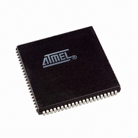
AT94K05AL-25AJI Atmel, AT94K05AL-25AJI Datasheet - Page 46

AT94K05AL-25AJI
Manufacturer Part Number
AT94K05AL-25AJI
Description
IC FPSLIC 5K GATE 25MHZ 84PLCC
Manufacturer
Atmel
Series
FPSLIC®r
Specifications of AT94K05AL-25AJI
Core Type
8-bit AVR
Speed
25MHz
Interface
I²C, UART
Program Sram Bytes
4K-16K
Fpga Sram
2kb
Data Sram Bytes
4K ~ 16K
Fpga Core Cells
256
Fpga Gates
5K
Fpga Registers
436
Voltage - Supply
3 V ~ 3.6 V
Mounting Type
Surface Mount
Operating Temperature
-40°C ~ 85°C
Package / Case
84-PLCC
For Use With
ATSTK594 - BOARD FPSLIC DAUGHTER FOR STK500
Lead Free Status / RoHS Status
Contains lead / RoHS non-compliant
Eeprom Size
-
Available stocks
Company
Part Number
Manufacturer
Quantity
Price
- Current page: 46 of 204
- Download datasheet (4Mb)
Data Direct
A 16-bit data address is contained in the 16 LSBs of a two-word instruction. Rd/Rr specify the
destination or source register.
Data Indirect with Displacement
Operand address is the result of the Y- or Z-register contents added to the address contained in
6 bits of the instruction word.
Data Indirect
Operand address is the contents of the X-, Y- or the Z-register.
Data Indirect with Pre-decrement
The X-, Y- or the Z-register is decremented before the operation. Operand address is the decre-
mented contents of the X, Y or the Z-register.
Data Indirect with Post-increment
The X-, Y- or the Z-register is incremented after the operation. The operand address is the con-
tent of the X-, Y- or the Z-register prior to incrementing.
Direct Program Address, JMP and CALL
Program execution continues at the address immediate in the instruction words.
Indirect Program Addressing, IJMP and ICALL
Program execution continues at address contained by the Z-register (i.e., the PC is loaded with
the contents of the Z-register).
Relative Program Addressing, RJMP and RCALL
Program execution continues at address PC + k + 1. The relative address k is -2048 to 2047.
4.10.2
Memory Access Times and Instruction Execution Timing
This section describes the general access timing concepts for instruction execution and internal
memory access.
The AVR CPU is driven by the XTAL1 input directly generated from the external clock crystal for
the chip. No internal clock division is used.
Figure 4-6
shows the parallel instruction fetches and instruction executions enabled by the Har-
vard architecture and the fast-access register file concept. This is the basic pipelining concept to
obtain up to 1 MIPS per MHz with the corresponding unique results for functions per cost, func-
tions per clocks and functions per power-unit.
AT94KAL Series FPSLIC
46
1138I–FPSLI–1/08
Related parts for AT94K05AL-25AJI
Image
Part Number
Description
Manufacturer
Datasheet
Request
R

Part Number:
Description:
IC FPSLIC 5K GATE 25MHZ 84PLCC
Manufacturer:
Atmel
Datasheet:

Part Number:
Description:
Fpslic Devices Combine 5K Gates of Atmel's Patented AT40K Fpga Architecture, a 20 Mips Avr 8-bit Risc Microprocessor Core, Numerous Fixed Microcontroller Peripheries And up to 36K Bytes of Program And Data SRAM.
Manufacturer:
ATMEL Corporation
Datasheet:

Part Number:
Description:
IC FPSLIC 5K GATE 25MHZ 208PQFP
Manufacturer:
Atmel
Datasheet:

Part Number:
Description:
IC FPSLIC 5K GATE 25MHZ 144LQFP
Manufacturer:
Atmel
Datasheet:

Part Number:
Description:
IC FPSLIC 5K GATE 25MHZ 208PQFP
Manufacturer:
Atmel
Datasheet:

Part Number:
Description:
IC FPSLIC 5K GATE 25MHZ 144LQFP
Manufacturer:
Atmel
Datasheet:

Part Number:
Description:
IC FPSLIC 5K GATE 25MHZ 144-LQFP
Manufacturer:
Atmel
Datasheet:

Part Number:
Description:
IC FPSLIC 5K GATE 25MHZ 100-TQFP
Manufacturer:
Atmel
Datasheet:

Part Number:
Description:
Manufacturer:
Atmel
Datasheet:

Part Number:
Description:
Manufacturer:
Atmel
Datasheet:

Part Number:
Description:
Manufacturer:
Atmel
Datasheet:

Part Number:
Description:
5k - 40k Gates Of At40k Fpga With 8-bit Microcontroller, Up To 36k Bytes Of Sram And On-chip Jtag Ice
Manufacturer:
ATMEL Corporation
Datasheet:

Part Number:
Description:
At94k05al 5k - 40k Gates Of At40k Fpga With 8-bit Microcontroller, Up To 36k Bytes Of Sram And On-chip Jtag Ice
Manufacturer:
ATMEL Corporation
Datasheet:

Part Number:
Description:
DEV KIT FOR AVR/AVR32
Manufacturer:
Atmel
Datasheet:


