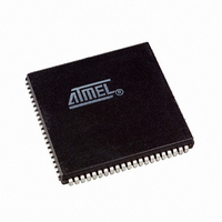
AT94K05AL-25AJI Atmel, AT94K05AL-25AJI Datasheet - Page 30

AT94K05AL-25AJI
Manufacturer Part Number
AT94K05AL-25AJI
Description
IC FPSLIC 5K GATE 25MHZ 84PLCC
Manufacturer
Atmel
Series
FPSLIC®r
Specifications of AT94K05AL-25AJI
Core Type
8-bit AVR
Speed
25MHz
Interface
I²C, UART
Program Sram Bytes
4K-16K
Fpga Sram
2kb
Data Sram Bytes
4K ~ 16K
Fpga Core Cells
256
Fpga Gates
5K
Fpga Registers
436
Voltage - Supply
3 V ~ 3.6 V
Mounting Type
Surface Mount
Operating Temperature
-40°C ~ 85°C
Package / Case
84-PLCC
For Use With
ATSTK594 - BOARD FPSLIC DAUGHTER FOR STK500
Lead Free Status / RoHS Status
Contains lead / RoHS non-compliant
Eeprom Size
-
Available stocks
Company
Part Number
Manufacturer
Quantity
Price
- Current page: 30 of 204
- Download datasheet (4Mb)
3.7
3.7.1
3.7.2
30
System Control
AT94KAL Series FPSLIC
Configuration Modes
System Control Register – FPGA/AVR
The AT94K family has four configuration modes controlled by mode pins M0 and M2, see
3-6.
Table 3-6.
Modes 2 and 3 are reserved and are used for factory test.
Modes 0 and 1 are pin-compatible with the appropriate AT40K counterpart. AVR I/O will be
taken over by the configuration logic for the CHECK pin during both modes.
Refer to the “AT94K Series Configuration” application note for details on downloading
bitstreams.
The configuration control register in the FPSLIC consists of 8 bytes of data, which are loaded
with the FPGA/Prog. Code at power-up from external nonvolatile memory. FPSLIC System Con-
trol Register values, see
defaults are included in the software.
Table 3-7.
M2
0
0
1
1
Bit
SCR0 - SCR1
SCR2
SCR3
SCR4
Configuration Modes
FPSLIC System Control Register
Description
Reserved
0 = Enable Cascading
1 = Disable Cascading
SCR2 controls the operation of the dual-function I/O CSOUT. When SCR2 is set,
the CSOUT pin is not used by the configuration during downloads, set this bit for
configurations where two or more devices are cascaded together. This applies for
configuration to another FPSLIC device or to an FPGA.
0 = Check Function Enabled
1 = Check Function Disabled
SCR3 controls the operation of the CHECK pin and enables the Check Function.
When SCR3 is set, the dual use AVR I/O/CHECK pin is not used by the
configuration during downloads, and can be used as AVR I/O.
0 = Memory Lockout Disabled
1 = Memory Lockout Enabled
SCR4 is the Security Flag and controls the writing and checking of configuration
memory during any subsequent configuration download. When SCR4 is set, any
subsequent configuration download initiated by the user, whether a normal
download or a CHECK function download, causes the INIT pin to immediately
activate. CON is released, and no further configuration activity takes place. The
download sequence during which SCR4 is set is NOT affected. The Control
Register write is also prohibited, so bit SCR4 may only be cleared by a power-on
reset or manual reset.
M0
0
1
0
1
Table
3-7, can be set in the System Designer software. Recommended
Name
Mode 0 - Master Serial
Mode 1 - Slave Serial Cascade
Mode 2 - Reserved
Mode 3 - Reserved
1138I–FPSLI–1/08
Table
Related parts for AT94K05AL-25AJI
Image
Part Number
Description
Manufacturer
Datasheet
Request
R

Part Number:
Description:
IC FPSLIC 5K GATE 25MHZ 84PLCC
Manufacturer:
Atmel
Datasheet:

Part Number:
Description:
Fpslic Devices Combine 5K Gates of Atmel's Patented AT40K Fpga Architecture, a 20 Mips Avr 8-bit Risc Microprocessor Core, Numerous Fixed Microcontroller Peripheries And up to 36K Bytes of Program And Data SRAM.
Manufacturer:
ATMEL Corporation
Datasheet:

Part Number:
Description:
IC FPSLIC 5K GATE 25MHZ 208PQFP
Manufacturer:
Atmel
Datasheet:

Part Number:
Description:
IC FPSLIC 5K GATE 25MHZ 144LQFP
Manufacturer:
Atmel
Datasheet:

Part Number:
Description:
IC FPSLIC 5K GATE 25MHZ 208PQFP
Manufacturer:
Atmel
Datasheet:

Part Number:
Description:
IC FPSLIC 5K GATE 25MHZ 144LQFP
Manufacturer:
Atmel
Datasheet:

Part Number:
Description:
IC FPSLIC 5K GATE 25MHZ 144-LQFP
Manufacturer:
Atmel
Datasheet:

Part Number:
Description:
IC FPSLIC 5K GATE 25MHZ 100-TQFP
Manufacturer:
Atmel
Datasheet:

Part Number:
Description:
Manufacturer:
Atmel
Datasheet:

Part Number:
Description:
Manufacturer:
Atmel
Datasheet:

Part Number:
Description:
Manufacturer:
Atmel
Datasheet:

Part Number:
Description:
5k - 40k Gates Of At40k Fpga With 8-bit Microcontroller, Up To 36k Bytes Of Sram And On-chip Jtag Ice
Manufacturer:
ATMEL Corporation
Datasheet:

Part Number:
Description:
At94k05al 5k - 40k Gates Of At40k Fpga With 8-bit Microcontroller, Up To 36k Bytes Of Sram And On-chip Jtag Ice
Manufacturer:
ATMEL Corporation
Datasheet:

Part Number:
Description:
DEV KIT FOR AVR/AVR32
Manufacturer:
Atmel
Datasheet:


