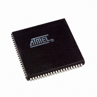
AT94K05AL-25AJI Atmel, AT94K05AL-25AJI Datasheet - Page 77

AT94K05AL-25AJI
Manufacturer Part Number
AT94K05AL-25AJI
Description
IC FPSLIC 5K GATE 25MHZ 84PLCC
Manufacturer
Atmel
Series
FPSLIC®r
Specifications of AT94K05AL-25AJI
Core Type
8-bit AVR
Speed
25MHz
Interface
I²C, UART
Program Sram Bytes
4K-16K
Fpga Sram
2kb
Data Sram Bytes
4K ~ 16K
Fpga Core Cells
256
Fpga Gates
5K
Fpga Registers
436
Voltage - Supply
3 V ~ 3.6 V
Mounting Type
Surface Mount
Operating Temperature
-40°C ~ 85°C
Package / Case
84-PLCC
For Use With
ATSTK594 - BOARD FPSLIC DAUGHTER FOR STK500
Lead Free Status / RoHS Status
Contains lead / RoHS non-compliant
Eeprom Size
-
Available stocks
Company
Part Number
Manufacturer
Quantity
Price
- Current page: 77 of 204
- Download datasheet (4Mb)
4.19.3
4.20
1138I–FPSLI–1/08
Bypass Register
Data Registers
ID-code of the device, since IDCODE is the default JTAG instruction. It may be desirable to have
the AVR device in reset during test mode. If not reset, inputs to the device may be determined by
the scan operations, and the internal software may be in an undetermined state when exiting the
test mode. If needed, the BYPASS instruction can be issued to make the shortest possible scan
chain through the device. The AVR can be set in the reset state either by pulling the external
AVR RESET pin Low, or issuing the AVR_RESET instruction with appropriate setting of the
Reset Data Register.
The EXTEST instruction is used for sampling external pins and loading output pins with data.
The data from the output latch will be driven out on the pins as soon as the EXTEST instruction
is loaded into the JTAG IR-register. Therefore, the SAMPLE/PRELOAD should also be used for
setting initial values to the scan ring, to avoid damaging the board when issuing the EXTEST
instruction for the first time. SAMPLE/PRELOAD can also be used for taking a snapshot of the
AVR’s external pins during normal operation of the part.
The JTAG Enable bit must be programmed and the JTD bit in the I/O register MCUR must be
cleared to enable the JTAG Test Access Port.
When using the JTAG interface for Boundary-Scan, using a JTAG TCK clock frequency higher
than the internal chip frequency is possible. The chip clock is not required to run.
The Data Registers are selected by the JTAG instruction registers described in section
ary-scan Specific JTAG Instructions” on page
operations are:
The Bypass register consists of a single shift-register stage. When the Bypass register is
selected as path between TDI and TDO, the register is reset to 0 when leaving the Capture-DR
controller state. The Bypass register can be used to shorten the scan chain on a system when
the other devices are to be tested.
• Bypass Register
• Device Identification Register
• AVR Reset Register
• AVR Boundary-Scan Chain
79. The data registers relevant for Boundary-Scan
AT94KAL Series FPSLIC
“Bound-
77
Related parts for AT94K05AL-25AJI
Image
Part Number
Description
Manufacturer
Datasheet
Request
R

Part Number:
Description:
IC FPSLIC 5K GATE 25MHZ 84PLCC
Manufacturer:
Atmel
Datasheet:

Part Number:
Description:
Fpslic Devices Combine 5K Gates of Atmel's Patented AT40K Fpga Architecture, a 20 Mips Avr 8-bit Risc Microprocessor Core, Numerous Fixed Microcontroller Peripheries And up to 36K Bytes of Program And Data SRAM.
Manufacturer:
ATMEL Corporation
Datasheet:

Part Number:
Description:
IC FPSLIC 5K GATE 25MHZ 208PQFP
Manufacturer:
Atmel
Datasheet:

Part Number:
Description:
IC FPSLIC 5K GATE 25MHZ 144LQFP
Manufacturer:
Atmel
Datasheet:

Part Number:
Description:
IC FPSLIC 5K GATE 25MHZ 208PQFP
Manufacturer:
Atmel
Datasheet:

Part Number:
Description:
IC FPSLIC 5K GATE 25MHZ 144LQFP
Manufacturer:
Atmel
Datasheet:

Part Number:
Description:
IC FPSLIC 5K GATE 25MHZ 144-LQFP
Manufacturer:
Atmel
Datasheet:

Part Number:
Description:
IC FPSLIC 5K GATE 25MHZ 100-TQFP
Manufacturer:
Atmel
Datasheet:

Part Number:
Description:
Manufacturer:
Atmel
Datasheet:

Part Number:
Description:
Manufacturer:
Atmel
Datasheet:

Part Number:
Description:
Manufacturer:
Atmel
Datasheet:

Part Number:
Description:
5k - 40k Gates Of At40k Fpga With 8-bit Microcontroller, Up To 36k Bytes Of Sram And On-chip Jtag Ice
Manufacturer:
ATMEL Corporation
Datasheet:

Part Number:
Description:
At94k05al 5k - 40k Gates Of At40k Fpga With 8-bit Microcontroller, Up To 36k Bytes Of Sram And On-chip Jtag Ice
Manufacturer:
ATMEL Corporation
Datasheet:

Part Number:
Description:
DEV KIT FOR AVR/AVR32
Manufacturer:
Atmel
Datasheet:


