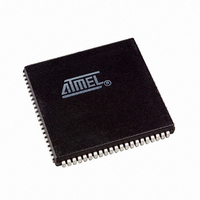
AT94K05AL-25AJI Atmel, AT94K05AL-25AJI Datasheet - Page 138

AT94K05AL-25AJI
Manufacturer Part Number
AT94K05AL-25AJI
Description
IC FPSLIC 5K GATE 25MHZ 84PLCC
Manufacturer
Atmel
Series
FPSLIC®r
Specifications of AT94K05AL-25AJI
Core Type
8-bit AVR
Speed
25MHz
Interface
I²C, UART
Program Sram Bytes
4K-16K
Fpga Sram
2kb
Data Sram Bytes
4K ~ 16K
Fpga Core Cells
256
Fpga Gates
5K
Fpga Registers
436
Voltage - Supply
3 V ~ 3.6 V
Mounting Type
Surface Mount
Operating Temperature
-40°C ~ 85°C
Package / Case
84-PLCC
For Use With
ATSTK594 - BOARD FPSLIC DAUGHTER FOR STK500
Lead Free Status / RoHS Status
Contains lead / RoHS non-compliant
Eeprom Size
-
Available stocks
Company
Part Number
Manufacturer
Quantity
Price
- Current page: 138 of 204
- Download datasheet (4Mb)
4.29.6
4.29.7
138
AT94KAL Series FPSLIC
Double Speed Transmission
The Baud-rate Generator in Double UART Speed Mode
UART0 Baud-rate Register Low Byte – UBRR0
UART1 Baud-rate Register Low Byte – UBRR1
UBRRn stores the 8 least significant bits of the UART baud-rate register.
The FPSLIC provides a separate UART mode that allows the user to double the communication
speed. By setting the U2X bit in UART Control and Status Register UCSRnA, the UART speed
will be doubled. The data reception will differ slightly from normal mode. Since the speed is dou-
bled, the receiver front-end logic samples the signals on the RXDn pin at a frequency 8 times the
baud-rate. While the line is idle, one single sample of logic 0 will be interpreted as the falling
edge of a start bit, and the start bit detection sequence is initiated. Let sample 1 denote the first
zero-sample. Following the 1-to-0 transition, the receiver samples the RXDn pin at samples 4, 5
and 6. If two or more of these three samples are found to be logic 1s, the start bit is rejected as
a noise spike and the receiver starts looking for the next 1-to-0 transition.
If however, a valid start bit is detected, sampling of the data bits following the start bit is per-
formed. These bits are also sampled at samples 4, 5 and 6. The logical value found in at least
two of the three samples is taken as the bit value. All bits are shifted into the transmitter shift reg-
ister as they are sampled. Sampling of an incoming character is shown in
Figure 4-44. Sampling Received Data when the Transmission Speed is Doubled
Note that the baud-rate equation is different from the equation
speed is doubled:
Note:
For standard crystal frequencies, the most commonly used baud-rates can be generated by
using the UBR settings in
than 1.5% from the target baud-rate, are bold in the table. However since the number of samples
Bit
$09 ($29)
Read/Write
Initial Value
Bit
$00 ($20)
Read/Write
Initial Value
• BAUD = Baud-rate
• f
• UBR = Contents of the UBRRHI and UBRRn Registers, (0 - 4095)
CK
SAMPLING
RECEIVER
= Crystal Clock Frequency
RXD
1. This equation is only valid when the UART transmission speed is doubled.
START BIT
7
MSB
R/W
0
7
MSB
R/W
0
D0
6
R/W
0
6
R/W
0
Table
D1
5
R/W
0
5
R/W
0
2. UBR values which yield an actual baud-rate differing less
BAUD
D2
4
R/W
0
4
R/W
0
=
----------------------------- -
8(UBR
D3
3
R/W
0
3
R/W
0
f
CK
+
D4
1 )
2
R/W
0
2
R/W
0
D5
(1)
at
1
R/W
0
1
R/W
0
page 136
D6
Figure
0
LSB
R/W
0
0
LSB
R/W
0
D7
when the UART
4-44.
1138I–FPSLI–1/08
STOP BIT
UBRR0
UBRR1
Related parts for AT94K05AL-25AJI
Image
Part Number
Description
Manufacturer
Datasheet
Request
R

Part Number:
Description:
IC FPSLIC 5K GATE 25MHZ 84PLCC
Manufacturer:
Atmel
Datasheet:

Part Number:
Description:
Fpslic Devices Combine 5K Gates of Atmel's Patented AT40K Fpga Architecture, a 20 Mips Avr 8-bit Risc Microprocessor Core, Numerous Fixed Microcontroller Peripheries And up to 36K Bytes of Program And Data SRAM.
Manufacturer:
ATMEL Corporation
Datasheet:

Part Number:
Description:
IC FPSLIC 5K GATE 25MHZ 208PQFP
Manufacturer:
Atmel
Datasheet:

Part Number:
Description:
IC FPSLIC 5K GATE 25MHZ 144LQFP
Manufacturer:
Atmel
Datasheet:

Part Number:
Description:
IC FPSLIC 5K GATE 25MHZ 208PQFP
Manufacturer:
Atmel
Datasheet:

Part Number:
Description:
IC FPSLIC 5K GATE 25MHZ 144LQFP
Manufacturer:
Atmel
Datasheet:

Part Number:
Description:
IC FPSLIC 5K GATE 25MHZ 144-LQFP
Manufacturer:
Atmel
Datasheet:

Part Number:
Description:
IC FPSLIC 5K GATE 25MHZ 100-TQFP
Manufacturer:
Atmel
Datasheet:

Part Number:
Description:
Manufacturer:
Atmel
Datasheet:

Part Number:
Description:
Manufacturer:
Atmel
Datasheet:

Part Number:
Description:
Manufacturer:
Atmel
Datasheet:

Part Number:
Description:
5k - 40k Gates Of At40k Fpga With 8-bit Microcontroller, Up To 36k Bytes Of Sram And On-chip Jtag Ice
Manufacturer:
ATMEL Corporation
Datasheet:

Part Number:
Description:
At94k05al 5k - 40k Gates Of At40k Fpga With 8-bit Microcontroller, Up To 36k Bytes Of Sram And On-chip Jtag Ice
Manufacturer:
ATMEL Corporation
Datasheet:

Part Number:
Description:
DEV KIT FOR AVR/AVR32
Manufacturer:
Atmel
Datasheet:


