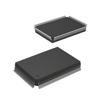
DF2357F20 Renesas Electronics America, DF2357F20 Datasheet - Page 292

DF2357F20
Manufacturer Part Number
DF2357F20
Description
IC H8S MCU FLASH 5V 128K 128QFP
Manufacturer
Renesas Electronics America
Series
H8® H8S/2300r
Datasheet
1.D12392F20V.pdf
(1049 pages)
Specifications of DF2357F20
Core Processor
H8S/2000
Core Size
16-Bit
Speed
20MHz
Connectivity
SCI, SmartCard
Peripherals
DMA, POR, PWM, WDT
Number Of I /o
87
Program Memory Size
128KB (128K x 8)
Program Memory Type
FLASH
Ram Size
8K x 8
Voltage - Supply (vcc/vdd)
4.5 V ~ 5.5 V
Data Converters
A/D 8x10b; D/A 2x8b
Oscillator Type
Internal
Operating Temperature
-20°C ~ 75°C
Package / Case
128-QFP
Lead Free Status / RoHS Status
Contains lead / RoHS non-compliant
Eeprom Size
-
Available stocks
Company
Part Number
Manufacturer
Quantity
Price
Company:
Part Number:
DF2357F20
Manufacturer:
Renesas Electronics America
Quantity:
10 000
Company:
Part Number:
DF2357F20IV
Manufacturer:
Renesas Electronics America
Quantity:
10 000
- Current page: 292 of 1049
- Download datasheet (5Mb)
The number of execution states is calculated from the formula below. Note that
by one activation event (the number in which the CHNE bit is set to 1, plus 1).
Number of execution states = I · S
For example, when the DTC vector address table is located in on-chip ROM, normal mode is set, and data is transferred
from the on-chip ROM to an internal I/O register, the time required for the DTC operation is 13 states. The time from
activation to the end of the data write is 10 states.
8.3.11
Activation by Interrupt: The procedure for using the DTC with interrupt activation is as follows:
[1] Set the MRA, MRB, SAR, DAR, CRA, and CRB register information in the on-chip RAM.
[2] Set the start address of the register information in the DTC vector address.
[3] Set the corresponding bit in DTCER to 1.
[4] Set the enable bits for the interrupt sources to be used as the activation sources to 1. The DTC is activated when an
[5] After the end of one data transfer, or after the specified number of data transfers have ended, the DTCE bit is cleared
Activation by Software: The procedure for using the DTC with software activation is as follows:
[1] Set the MRA, MRB, SAR, DAR, CRA, and CRB register information in the on-chip RAM.
[2] Set the start address of the register information in the DTC vector address.
[3] Check that the SWDTE bit is 0.
[4] Write 1 to SWDTE bit and the vector number to DTVECR.
[5] Check the vector number written to DTVECR.
[6] After the end of one data transfer, if the DISEL bit is 0 and a CPU interrupt is not requested, the SWDTE bit is
8.3.12
(1) Normal Mode
An example is shown in which the DTC is used to receive 128 bytes of data via the SCI.
[1] Set MRA to fixed source address (SM1 = SM0 = 0), incrementing destination address (DM1 = 1, DM0 = 0), normal
[2] Set the start address of the register information at the DTC vector address.
[3] Set the corresponding bit in DTCER to 1.
Rev.6.00 Oct.28.2004 page 262 of 1016
REJ09B0138-0600H
interrupt used as an activation source is generated.
to 0 and a CPU interrupt is requested. If the DTC is to continue transferring data, set the DTCE bit to 1.
cleared to 0. If the DTC is to continue transferring data, set the SWDTE bit to 1. When the DISEL bit is 1, or after the
specified number of data transfers have ended, the SWDTE bit is held at 1 and a CPU interrupt is requested.
mode (MD1 = MD0 = 0), and byte size (Sz = 0). The DTS bit can have any value. Set MRB for one data transfer by
one interrupt (CHNE = 0, DISEL = 0). Set the SCI RDR address in SAR, the start address of the RAM area where the
data will be received in DAR, and 128 (H'0080) in CRA. CRB can be set to any value.
Procedures for Using DTC
Examples of Use of the D7TC
I
+
(J · S
J
+ K · S
K
+ L · S
L
) + M · S
M
means the sum of all transfers activated
Related parts for DF2357F20
Image
Part Number
Description
Manufacturer
Datasheet
Request
R

Part Number:
Description:
KIT STARTER FOR M16C/29
Manufacturer:
Renesas Electronics America
Datasheet:

Part Number:
Description:
KIT STARTER FOR R8C/2D
Manufacturer:
Renesas Electronics America
Datasheet:

Part Number:
Description:
R0K33062P STARTER KIT
Manufacturer:
Renesas Electronics America
Datasheet:

Part Number:
Description:
KIT STARTER FOR R8C/23 E8A
Manufacturer:
Renesas Electronics America
Datasheet:

Part Number:
Description:
KIT STARTER FOR R8C/25
Manufacturer:
Renesas Electronics America
Datasheet:

Part Number:
Description:
KIT STARTER H8S2456 SHARPE DSPLY
Manufacturer:
Renesas Electronics America
Datasheet:

Part Number:
Description:
KIT STARTER FOR R8C38C
Manufacturer:
Renesas Electronics America
Datasheet:

Part Number:
Description:
KIT STARTER FOR R8C35C
Manufacturer:
Renesas Electronics America
Datasheet:

Part Number:
Description:
KIT STARTER FOR R8CL3AC+LCD APPS
Manufacturer:
Renesas Electronics America
Datasheet:

Part Number:
Description:
KIT STARTER FOR RX610
Manufacturer:
Renesas Electronics America
Datasheet:

Part Number:
Description:
KIT STARTER FOR R32C/118
Manufacturer:
Renesas Electronics America
Datasheet:

Part Number:
Description:
KIT DEV RSK-R8C/26-29
Manufacturer:
Renesas Electronics America
Datasheet:

Part Number:
Description:
KIT STARTER FOR SH7124
Manufacturer:
Renesas Electronics America
Datasheet:

Part Number:
Description:
KIT STARTER FOR H8SX/1622
Manufacturer:
Renesas Electronics America
Datasheet:

Part Number:
Description:
KIT DEV FOR SH7203
Manufacturer:
Renesas Electronics America
Datasheet:


