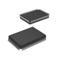
DF2357F20 Renesas Electronics America, DF2357F20 Datasheet - Page 578

DF2357F20
Manufacturer Part Number
DF2357F20
Description
IC H8S MCU FLASH 5V 128K 128QFP
Manufacturer
Renesas Electronics America
Series
H8® H8S/2300r
Datasheet
1.D12392F20V.pdf
(1049 pages)
Specifications of DF2357F20
Core Processor
H8S/2000
Core Size
16-Bit
Speed
20MHz
Connectivity
SCI, SmartCard
Peripherals
DMA, POR, PWM, WDT
Number Of I /o
87
Program Memory Size
128KB (128K x 8)
Program Memory Type
FLASH
Ram Size
8K x 8
Voltage - Supply (vcc/vdd)
4.5 V ~ 5.5 V
Data Converters
A/D 8x10b; D/A 2x8b
Oscillator Type
Internal
Operating Temperature
-20°C ~ 75°C
Package / Case
128-QFP
Lead Free Status / RoHS Status
Contains lead / RoHS non-compliant
Eeprom Size
-
Available stocks
Company
Part Number
Manufacturer
Quantity
Price
Company:
Part Number:
DF2357F20
Manufacturer:
Renesas Electronics America
Quantity:
10 000
Company:
Part Number:
DF2357F20IV
Manufacturer:
Renesas Electronics America
Quantity:
10 000
- Current page: 578 of 1049
- Download datasheet (5Mb)
16.4.2
Scan mode is useful for monitoring analog inputs in a group of one or more channels. When the ADST bit is set to 1 by a
software, timer or external trigger input, A/D conversion starts on the first channel in the group (AN0). When two or
more channels are selected, after conversion of the first channel ends, conversion of the second channel (AN1) starts
immediately. A/D conversion continues cyclically on the selected channels until the ADST bit is cleared to 0. The
conversion results are transferred for storage into the ADDR registers corresponding to the channels.
When the operating mode or analog input channel must be changed during analog conversion, to prevent incorrect
operation, first clear the ADST bit to 0 in ADCSR to halt A/D conversion. After making the necessary changes, set the
ADST bit to 1 to start A/D conversion again. The ADST bit can be set at the same time as the operating mode or input
channel is changed.
Typical operations when three channels (AN0 to AN2) are selected in scan mode are described next. Figure 16-4 shows a
timing diagram for this example.
[1] Scan mode is selected (SCAN = 1), scan group 0 is selected (CH2 = 0), analog input channels AN0 to AN2 are
[2] When A/D conversion of the first channel (AN0) is completed, the result is transferred to ADDRA. Next, conversion
[3] Conversion proceeds in the same way through the third channel (AN2).
[4] When conversion of all the selected channels (AN0 to AN2) is completed, the ADF flag is set to 1 and conversion of
[5] Steps [2] to [4] are repeated as long as the ADST bit remains set to 1. When the ADST bit is cleared to 0, A/D
Rev.6.00 Oct.28.2004 page 548 of 1016
REJ09B0138-0600H
selected (CH1 = 1, CH0 = 0), and A/D conversion is started (ADST = 1)
of the second channel (AN1) starts automatically.
the first channel (AN0) starts again. If the ADIE bit is set to 1 at this time, an ADI interrupt is requested after A/D
conversion ends.
conversion stops. After that, if the ADST bit is set to 1, A/D conversion starts again from the first channel (AN0).
Scan Mode (SCAN = 1)
State of channel 0 (AN0)
State of channel 1 (AN1)
State of channel 2 (AN2)
State of channel 3 (AN3)
Notes: 1. Vertical arrows ( ) indicate instructions executed by software.
ADDRA
ADDRB
ADDRC
ADDRD
ADST
ADF
2. Data currently being converted is ignored.
Idle
Figure 16-4 Example of A/D Converter Operation
(Scan Mode, Channels AN0 to AN2 Selected)
Idle
A/D conversion 1
Idle
Set*
1
A/D conversion 2
Transfer
Continuous A/D conversion execution
A/D conversion result 1
Idle
A/D conversion 3
Idle
Idle
A/D conversion 4
A/D conversion time
A/D conversion result 2
A/D conversion result 3
A/D conversion 5
A/D conversion result 4
Clear*
*
2
Idle
Idle
Idle
1
Clear*
1
Related parts for DF2357F20
Image
Part Number
Description
Manufacturer
Datasheet
Request
R

Part Number:
Description:
KIT STARTER FOR M16C/29
Manufacturer:
Renesas Electronics America
Datasheet:

Part Number:
Description:
KIT STARTER FOR R8C/2D
Manufacturer:
Renesas Electronics America
Datasheet:

Part Number:
Description:
R0K33062P STARTER KIT
Manufacturer:
Renesas Electronics America
Datasheet:

Part Number:
Description:
KIT STARTER FOR R8C/23 E8A
Manufacturer:
Renesas Electronics America
Datasheet:

Part Number:
Description:
KIT STARTER FOR R8C/25
Manufacturer:
Renesas Electronics America
Datasheet:

Part Number:
Description:
KIT STARTER H8S2456 SHARPE DSPLY
Manufacturer:
Renesas Electronics America
Datasheet:

Part Number:
Description:
KIT STARTER FOR R8C38C
Manufacturer:
Renesas Electronics America
Datasheet:

Part Number:
Description:
KIT STARTER FOR R8C35C
Manufacturer:
Renesas Electronics America
Datasheet:

Part Number:
Description:
KIT STARTER FOR R8CL3AC+LCD APPS
Manufacturer:
Renesas Electronics America
Datasheet:

Part Number:
Description:
KIT STARTER FOR RX610
Manufacturer:
Renesas Electronics America
Datasheet:

Part Number:
Description:
KIT STARTER FOR R32C/118
Manufacturer:
Renesas Electronics America
Datasheet:

Part Number:
Description:
KIT DEV RSK-R8C/26-29
Manufacturer:
Renesas Electronics America
Datasheet:

Part Number:
Description:
KIT STARTER FOR SH7124
Manufacturer:
Renesas Electronics America
Datasheet:

Part Number:
Description:
KIT STARTER FOR H8SX/1622
Manufacturer:
Renesas Electronics America
Datasheet:

Part Number:
Description:
KIT DEV FOR SH7203
Manufacturer:
Renesas Electronics America
Datasheet:


