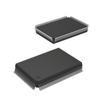
DF2357F20 Renesas Electronics America, DF2357F20 Datasheet - Page 983

DF2357F20
Manufacturer Part Number
DF2357F20
Description
IC H8S MCU FLASH 5V 128K 128QFP
Manufacturer
Renesas Electronics America
Series
H8® H8S/2300r
Datasheet
1.D12392F20V.pdf
(1049 pages)
Specifications of DF2357F20
Core Processor
H8S/2000
Core Size
16-Bit
Speed
20MHz
Connectivity
SCI, SmartCard
Peripherals
DMA, POR, PWM, WDT
Number Of I /o
87
Program Memory Size
128KB (128K x 8)
Program Memory Type
FLASH
Ram Size
8K x 8
Voltage - Supply (vcc/vdd)
4.5 V ~ 5.5 V
Data Converters
A/D 8x10b; D/A 2x8b
Oscillator Type
Internal
Operating Temperature
-20°C ~ 75°C
Package / Case
128-QFP
Lead Free Status / RoHS Status
Contains lead / RoHS non-compliant
Eeprom Size
-
Available stocks
Company
Part Number
Manufacturer
Quantity
Price
Company:
Part Number:
DF2357F20
Manufacturer:
Renesas Electronics America
Quantity:
10 000
Company:
Part Number:
DF2357F20IV
Manufacturer:
Renesas Electronics America
Quantity:
10 000
- Current page: 983 of 1049
- Download datasheet (5Mb)
TIOR0L—Timer I/O Control Register 0L
Note: When TGRC or TGRD is designated for buffer operation, this setting is invalid and the register operates as a buffer register.
Bit
Initial value
Read/Write
Notes: 1. When bits TPSC2 to TPSC0 in TCR1 are set to B'000, and ø/1 is used as
TGR0D I/O Control
:
:
:
:
0
1
IOD3
R/W
7
0
0
1
0
1
2. When the BFB bit in TMDR0 is set to 1 and TGR0D is used as a buffer
the TCNT1 count clock, this setting is invalid and input capture is not
generated.
register, this setting is invalid and input capture/output compare is not
generated.
0
1
0
1
0
1
IOD2
R/W
0
1
0
1
0
1
0
1
0
1
6
0
TGR0D
is output
compare
register
*
TGR0D
is input
capture
register
*
2
2
IOD1
R/W
5
0
Output disabled
Initial output is
0 output
Output disabled
Initial output is
1 output
Capture input
source is
TIOCD0 pin
Capture input
source is channel
1/count clock
Note: When the BFA bit in TMDR0 is set to 1 and TGR0C is used as a buffer
IOD0
TGR0C I/O Control
R/W
0
1
4
0
register, this setting is invalid and input capture/output compare is not
generated.
0
1
0
1
H'FFD3
IOC3
R/W
0
1
0
1
0
1
3
0
0 output at compare match
1 output at compare match
Toggle output at compare match
0 output at compare match
1 output at compare match
Toggle output at compare match
Input capture at rising edge
Input capture at falling edge
Input capture at both edges
Input capture at TCNT1 count-up/
count-down
0
1
0
1
0
1
0
1
0
1
TGR0C
is output
compare
register
TGR0C
is input
capture
register
IOC2
R/W
2
0
*
1
Output disabled
Initial output is
0 output
Output disabled
Initial output is
1 output
Capture input
source is
TIOCC0 pin
Capture input
source is channel
1/count clock
IOC1
R/W
1
0
: Don’t care
IOC0
R/W
0
0
0 output at compare match
1 output at compare match
Toggle output at compare match
0 output at compare match
1 output at compare match
Toggle output at compare match
Input capture at rising edge
Input capture at falling edge
Input capture at both edges
Input capture at TCNT1 count-up/
count-down
Rev.6.00 Oct.28.2004 page 953 of 1016
TPU0
: Don’t care
REJ09B0138-0600H
Related parts for DF2357F20
Image
Part Number
Description
Manufacturer
Datasheet
Request
R

Part Number:
Description:
KIT STARTER FOR M16C/29
Manufacturer:
Renesas Electronics America
Datasheet:

Part Number:
Description:
KIT STARTER FOR R8C/2D
Manufacturer:
Renesas Electronics America
Datasheet:

Part Number:
Description:
R0K33062P STARTER KIT
Manufacturer:
Renesas Electronics America
Datasheet:

Part Number:
Description:
KIT STARTER FOR R8C/23 E8A
Manufacturer:
Renesas Electronics America
Datasheet:

Part Number:
Description:
KIT STARTER FOR R8C/25
Manufacturer:
Renesas Electronics America
Datasheet:

Part Number:
Description:
KIT STARTER H8S2456 SHARPE DSPLY
Manufacturer:
Renesas Electronics America
Datasheet:

Part Number:
Description:
KIT STARTER FOR R8C38C
Manufacturer:
Renesas Electronics America
Datasheet:

Part Number:
Description:
KIT STARTER FOR R8C35C
Manufacturer:
Renesas Electronics America
Datasheet:

Part Number:
Description:
KIT STARTER FOR R8CL3AC+LCD APPS
Manufacturer:
Renesas Electronics America
Datasheet:

Part Number:
Description:
KIT STARTER FOR RX610
Manufacturer:
Renesas Electronics America
Datasheet:

Part Number:
Description:
KIT STARTER FOR R32C/118
Manufacturer:
Renesas Electronics America
Datasheet:

Part Number:
Description:
KIT DEV RSK-R8C/26-29
Manufacturer:
Renesas Electronics America
Datasheet:

Part Number:
Description:
KIT STARTER FOR SH7124
Manufacturer:
Renesas Electronics America
Datasheet:

Part Number:
Description:
KIT STARTER FOR H8SX/1622
Manufacturer:
Renesas Electronics America
Datasheet:

Part Number:
Description:
KIT DEV FOR SH7203
Manufacturer:
Renesas Electronics America
Datasheet:


