EM357-MOD-LR-ANT-TG Ember, EM357-MOD-LR-ANT-TG Datasheet - Page 127
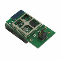
EM357-MOD-LR-ANT-TG
Manufacturer Part Number
EM357-MOD-LR-ANT-TG
Description
MODULE EM357 PA/LNA W/ANT TG
Manufacturer
Ember
Specifications of EM357-MOD-LR-ANT-TG
Frequency
2.4GHz
Data Rate - Maximum
250kbps
Modulation Or Protocol
802.15.4 Zigbee
Voltage - Supply
2.1 V ~ 3.6 V
Current - Receiving
25mA
Current - Transmitting
42mA
Data Interface
PCB, Surface Mount
Memory Size
192kB Flash, 12kB RAM
Antenna Connector
On-Board, Chip
Operating Temperature
-40°C ~ 85°C
Package / Case
Module
Lead Free Status / RoHS Status
Lead free / RoHS Compliant
Power - Output
-
Applications
-
Sensitivity
-
Other names
636-1020


9.2 GPIO Usage
9.3 Timer Functional Description
The timers can optionally use GPIOs in the PA and PB ports for external inputs or outputs. As with all EM35x
digital inputs, a GPIO used as a timer input can be shared with other uses of the same pin. Available timer
inputs include an external timer clock, a clock mask, and four input channels. Any GPIO used as a timer output
must be configured as an alternate output and is controlled only by the timer.
Many of the GPIOs that can be assigned as timer outputs can also be used by another on-chip peripheral such
as a serial controller. Using a GPIO as a timer output takes precedence over another peripheral function, as
long as the channel is configured as an output in the TIMx_CCMR1 register and is enabled in the TIMx_CCER
register.
The GPIOs that can be used by Timer 1 are fixed, but the GPIOs that can be used as Timer 2 channels can be
mapped to either of two pins, as shown in Table 9-1. The Timer 2 Option Register (TIM2_OR) has four single
bit fields (TIM_REMAPCy) that control whether a Timer 2 channel is mapped to its default GPIO in port PA, or
remapped to a GPIO in PB.
Table 9-1 specifies the pins that may be assigned to Timer 1 and Timer 2 functions.
The TIMxCLK and TIMxMSK inputs can be used only in the external clock modes; refer to the External Clock
Source Mode 1 and External Clock Source Mode 2 sections for details concerning their use.
9.3.1
The main block of the general purpose timer is a 16-bit counter with its related auto-reload register. The
counter can count up, down, or alternate up and down. The counter clock can be divided by a prescaler.
The counter, the auto-reload register, and the prescaler register can be written to or read by software. This is
true even when the counter is running.
The time-base unit includes:
Some timer registers cannot be directly accessed by software, which instead reads and writes a “buffer
register”. The internal registers actually used for timer operations are called “shadow registers”.
The auto-reload register is buffered. Writing to or reading from the auto-reload register accesses the buffer
register. The contents of the buffer register are transferred into the shadow register permanently or at each
Timer 1
Timer 2
(TIM_REMAPCy = 0)
Timer 2
(TIM_REMAPCy = 1)
Counter Register (TIMx_CNT)
Prescaler Register (TIMx_PSC)
Auto-Reload Register (TIMx_ARR)
(direction)
Signal
Time-Base Unit
(in or out)
TIMxC1
PB6
PA0
PB1
(in or out)
TIMxC2
Table 9-1. Timer GPIO Usage
PB7
PA3
PB2
Final
9-3
(in or out)
TIMxC3
PA6
PA1
PB3
(in or out)
TIMxC4
PA7
PA2
PB4
EM351 / EM357
TIMxCLK
PB0
PB5
PB5
(in)
120-035X-000G
TIMxMSK
PB5
PB0
PB0
(in)
Related parts for EM357-MOD-LR-ANT-TG
Image
Part Number
Description
Manufacturer
Datasheet
Request
R

Part Number:
Description:
MODULE EM357 NO PA/LNA W/ANT TG
Manufacturer:
Ember
Datasheet:

Part Number:
Description:
MODULE EM357 NO PA/LNA W/RF CONN
Manufacturer:
Ember
Datasheet:
Part Number:
Description:
MODULE EM357 PA/LNA W/RF CONN
Manufacturer:
Ember
Datasheet:

Part Number:
Description:
KIT DEV EMBER ZIGBEE W/PCWH
Manufacturer:
Custom Computer Services Inc (CCS)

Part Number:
Description:
PROGRAMMER USB FLASH EM250/260
Manufacturer:
Ember
Datasheet:

Part Number:
Description:
IC ZIGBEE SYSTEM-ON-CHIP 40-QFN
Manufacturer:
Ember
Datasheet:

Part Number:
Description:
IC ZIGBEE SYSTEM-ON-CHIP 48-QFN
Manufacturer:
Ember
Datasheet:
Part Number:
Description:
IC RF TXRX ZIGBEE 128KB 48QFN
Manufacturer:
Ember
Datasheet:
Part Number:
Description:
IC RF TXRX ZIGBEE 192KB 48QFN
Manufacturer:
Ember
Datasheet:

Part Number:
Description:
INSIGHT ADAPTER FOR EM2XX
Manufacturer:
Ember
Datasheet:

Part Number:
Description:
IAR EWARM LICENCE FOR EM35X
Manufacturer:
Ember
Datasheet:

Part Number:
Description:
KIT EVAL EM250 RF TEST
Manufacturer:
Ember
Datasheet:

Part Number:
Description:
INSIGHT ADAPTER 3 FOR EM35X
Manufacturer:
Ember
Datasheet:

Part Number:
Description:
EM250 RCM BOARD
Manufacturer:
Ember
Datasheet:

Part Number:
Description:
EM35X BREAKOUT BOARD
Manufacturer:
Ember
Datasheet: