EM357-MOD-LR-ANT-TG Ember, EM357-MOD-LR-ANT-TG Datasheet - Page 56
EM357-MOD-LR-ANT-TG
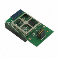
Manufacturer Part Number
EM357-MOD-LR-ANT-TG
Description
MODULE EM357 PA/LNA W/ANT TG
Manufacturer
Ember
Specifications of EM357-MOD-LR-ANT-TG
Frequency
2.4GHz
Data Rate - Maximum
250kbps
Modulation Or Protocol
802.15.4 Zigbee
Voltage - Supply
2.1 V ~ 3.6 V
Current - Receiving
25mA
Current - Transmitting
42mA
Data Interface
PCB, Surface Mount
Memory Size
192kB Flash, 12kB RAM
Antenna Connector
On-Board, Chip
Operating Temperature
-40°C ~ 85°C
Package / Case
Module
Lead Free Status / RoHS Status
Lead free / RoHS Compliant
Power - Output
-
Applications
-
Sensitivity
-
Other names
636-1020


7.3
Forced Functions
For outputs assigned to the serial controllers, the serial interface mode registers (SCx_MODE) determine how
the GPIO pins are used.
The alternate outputs of PA4 and PA5 can either provide packet trace data (PTI_EN and PTI_DATA), or
synchronous CPU trace data (TRACEDATA2 and TRACEDATA3). The selection of packet trace or CPU trace is
made through the Ember software.
If a GPIO does not have an associated peripheral in alternate output mode, its output is set to 0.
For some GPIOs the GPIO_PxCFGH/L configuration will be overridden. These functions are forced when the
EM35x is reset and remain forced until software overrides the forced functions. Table 7-3 shows the GPIOs
that have different functions forced on them regardless of the GPIO_PxCFGH/L registers.
1
PA7 is forced to be the regulator enable signal, REG_EN. If an external regulator is used and controlled
through REG_EN, PA7’s forced functionality must not be overridden. If an external regulator is not used,
REG_EN may be disabled and PA7 may be reclaimed as a normal GPIO. Disabling REG_EN is done by clearing
the bit GPIO_EXTREGEN in the GPIO_DBGCFG register.
PC0, PC2, PC3, and PC4 are forced to be the Serial Wire and JTAG (SWJ) Interface. When the EM35x resets,
these four GPIOs are forced to operate in JTAG mode. Switching the debug interface between JTAG mode and
Serial Wire mode can only be accomplished by the external debug tool and cannot be affected by software
executing on the EM35x. Due to the fact that Serial Wire mode can only be invoked by an external debug tool
Timer 2 Output
TIM2C1
TIM2C2
TIM2C3
TIM2C4
GPIO Forced Mode
PA7
PC0
PC2
PC3
PC4
PC4
and SWDIO is forced when the SWJ is in Serial Wire mode.
The choice of PC4’s forced signal is controlled by an external debug tool. JTMS is forced when the SWJ is in JTAG mode
1
1
Open-drain output
Input with pull up
Push-pull output
Input with pull up
Input with pull up
Bidirectional (push-pull output or floating input) controlled by debugger interface SWDIO
Option Register Bit
TIM2_OR[4]
TIM2_OR[5]
TIM2_OR[6]
TIM2_OR[7]
Table 7-2. Timer 2 Output Configuration Controls
Table 7-3. GPIO Forced Functions
Final
7-3
GPIO Mapping Selected by TIM2_OR Bit
PA0
PA3
PA1
PA2
0
EM351 / EM357
Forced Signal
REG_EN
JRST
JTDO
JDTI
JTMS
PB1
PB2
PB3
PB4
1
120-035X-000G
Related parts for EM357-MOD-LR-ANT-TG
Image
Part Number
Description
Manufacturer
Datasheet
Request
R

Part Number:
Description:
MODULE EM357 NO PA/LNA W/ANT TG
Manufacturer:
Ember
Datasheet:

Part Number:
Description:
MODULE EM357 NO PA/LNA W/RF CONN
Manufacturer:
Ember
Datasheet:
Part Number:
Description:
MODULE EM357 PA/LNA W/RF CONN
Manufacturer:
Ember
Datasheet:

Part Number:
Description:
KIT DEV EMBER ZIGBEE W/PCWH
Manufacturer:
Custom Computer Services Inc (CCS)

Part Number:
Description:
PROGRAMMER USB FLASH EM250/260
Manufacturer:
Ember
Datasheet:

Part Number:
Description:
IC ZIGBEE SYSTEM-ON-CHIP 40-QFN
Manufacturer:
Ember
Datasheet:

Part Number:
Description:
IC ZIGBEE SYSTEM-ON-CHIP 48-QFN
Manufacturer:
Ember
Datasheet:
Part Number:
Description:
IC RF TXRX ZIGBEE 128KB 48QFN
Manufacturer:
Ember
Datasheet:
Part Number:
Description:
IC RF TXRX ZIGBEE 192KB 48QFN
Manufacturer:
Ember
Datasheet:

Part Number:
Description:
INSIGHT ADAPTER FOR EM2XX
Manufacturer:
Ember
Datasheet:

Part Number:
Description:
IAR EWARM LICENCE FOR EM35X
Manufacturer:
Ember
Datasheet:

Part Number:
Description:
KIT EVAL EM250 RF TEST
Manufacturer:
Ember
Datasheet:

Part Number:
Description:
INSIGHT ADAPTER 3 FOR EM35X
Manufacturer:
Ember
Datasheet:

Part Number:
Description:
EM250 RCM BOARD
Manufacturer:
Ember
Datasheet:

Part Number:
Description:
EM35X BREAKOUT BOARD
Manufacturer:
Ember
Datasheet: