EM357-MOD-LR-ANT-TG Ember, EM357-MOD-LR-ANT-TG Datasheet - Page 185
EM357-MOD-LR-ANT-TG
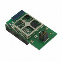
Manufacturer Part Number
EM357-MOD-LR-ANT-TG
Description
MODULE EM357 PA/LNA W/ANT TG
Manufacturer
Ember
Specifications of EM357-MOD-LR-ANT-TG
Frequency
2.4GHz
Data Rate - Maximum
250kbps
Modulation Or Protocol
802.15.4 Zigbee
Voltage - Supply
2.1 V ~ 3.6 V
Current - Receiving
25mA
Current - Transmitting
42mA
Data Interface
PCB, Surface Mount
Memory Size
192kB Flash, 12kB RAM
Antenna Connector
On-Board, Chip
Operating Temperature
-40°C ~ 85°C
Package / Case
Module
Lead Free Status / RoHS Status
Lead free / RoHS Compliant
Power - Output
-
Applications
-
Sensitivity
-
Other names
636-1020


10.3
Operation
Bits in INT_ADCFLAG register may be cleared by writing a 1 to their position. Writing 0 to any bit in the
INT_ADCFLAG register is ineffectual.
The INT_ADCCFG register controls whether or not INT_ADCFLAG register bits actually propagate the ADC
interrupt to the NVIC. Only the events whose bits are 1 in the INT_ADCCFG register can do so.
For non-interrupt (polled) ADC operation set the INT_ADCCFG register to zero, and read the bit flags in the
INT_ADCFLAG register to determine the ADC status.
Note: When making changes to the ADC configuration it is best to disable the DMA beforehand. If this isn’t
done it can be difficult to determine at which point the sampled data in the DMA buffer switched from the old
configuration to the new configuration. However, since the ADC will be left running, if it completes a
conversion after the DMA is disabled, the INT_ADCOVF flag will be set. To prevent these unwanted DMA buffer
overflow indications, clear the INT_ADCOVF flag immediately after enabling the DMA, preferably with
interrupts off. Disabling the ADC in addition to the DMA is often undesirable because of the additional analog
startup time when it is re-enabled.
Setting the ADC_EN bit in the ADC_CFG register enables the ADC. Once the ADC is enabled, it performs
conversions continuously until it is disabled. If the ADC had previously been disabled, a 21 µs analog startup
delay is automatically imposed before the ADC starts conversions. The delay timing is performed in hardware
and is simply added to the time until the first conversion result is output.
When the ADC is first enabled, and/or if any change is made to ADC_CFG after it is enabled, the time until a
result is output is double the normal sample time. This is because the ADC’s internal design requires it to
discard the first conversion after startup or a configuration change. This is done automatically and is hidden
from software. Switching the system clock between OSCHF and OSC24M also causes the ADC to go through this
startup cycle. If the ADC was newly enabled, the analog delay time is added to the doubled sample time.
If the DMA is running when the ADC_CFG register is modified, the DMA does not stop, so the DMA buffer may
contain conversion results from both the old and new configurations.
The following procedure illustrates a simple polled method of using the ADC without DMA. This assumes that
any GPIOs and the voltage reference have already been configured.
1.
2.
3.
4.
5.
The following procedure illustrates a simple polled method of using the ADC with DMA. After completing the
procedure, the latest conversion results are available in the location written to by the DMA. This assumes that
any GPIOs and the voltage reference have already been configured.
1.
2.
INT_ADCULDFULL – the DMA wrote to the last location in the buffer (DMA buffer full).
INT_ADCULDHALF – the DMA wrote to the last location of the first half of the DMA buffer (DMA buffer half
full).
INT_ADCDATA – there is data ready in the ADC_DATA register.
Disable all ADC interrupts: Write 0 to the INT_ADCCFG register.
Write the desired offset and gain correction values to the ADC_OFFSET and ADC_GAIN registers.
Write the desired conversion configuration, with the ADC_EN bit set, to ADC_CFG register.
Clear the ADC data flag: Write the INT_ADCDATA bit to INT_ADCFLAG register.
Wait until the INT_ADCDATA bit is set in INT_ADCFLAG register, then read the result, as a 16-bit signed
variable, from the ADC_DATA register.
Allocate a 16-bit signed variable, for example analogData, to receive the ADC output.
(Make sure that analogData is half-word aligned – that is, at an even address.)
Disable all ADC interrupts: Write 0 to the INT_ADCCFG register.
Final
10-6
EM351 / EM357
120-035X-000G
Related parts for EM357-MOD-LR-ANT-TG
Image
Part Number
Description
Manufacturer
Datasheet
Request
R

Part Number:
Description:
MODULE EM357 NO PA/LNA W/ANT TG
Manufacturer:
Ember
Datasheet:

Part Number:
Description:
MODULE EM357 NO PA/LNA W/RF CONN
Manufacturer:
Ember
Datasheet:
Part Number:
Description:
MODULE EM357 PA/LNA W/RF CONN
Manufacturer:
Ember
Datasheet:

Part Number:
Description:
KIT DEV EMBER ZIGBEE W/PCWH
Manufacturer:
Custom Computer Services Inc (CCS)

Part Number:
Description:
PROGRAMMER USB FLASH EM250/260
Manufacturer:
Ember
Datasheet:

Part Number:
Description:
IC ZIGBEE SYSTEM-ON-CHIP 40-QFN
Manufacturer:
Ember
Datasheet:

Part Number:
Description:
IC ZIGBEE SYSTEM-ON-CHIP 48-QFN
Manufacturer:
Ember
Datasheet:
Part Number:
Description:
IC RF TXRX ZIGBEE 128KB 48QFN
Manufacturer:
Ember
Datasheet:
Part Number:
Description:
IC RF TXRX ZIGBEE 192KB 48QFN
Manufacturer:
Ember
Datasheet:

Part Number:
Description:
INSIGHT ADAPTER FOR EM2XX
Manufacturer:
Ember
Datasheet:

Part Number:
Description:
IAR EWARM LICENCE FOR EM35X
Manufacturer:
Ember
Datasheet:

Part Number:
Description:
KIT EVAL EM250 RF TEST
Manufacturer:
Ember
Datasheet:

Part Number:
Description:
INSIGHT ADAPTER 3 FOR EM35X
Manufacturer:
Ember
Datasheet:

Part Number:
Description:
EM250 RCM BOARD
Manufacturer:
Ember
Datasheet:

Part Number:
Description:
EM35X BREAKOUT BOARD
Manufacturer:
Ember
Datasheet: