EM357-MOD-LR-ANT-TG Ember, EM357-MOD-LR-ANT-TG Datasheet - Page 42
EM357-MOD-LR-ANT-TG
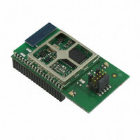
Manufacturer Part Number
EM357-MOD-LR-ANT-TG
Description
MODULE EM357 PA/LNA W/ANT TG
Manufacturer
Ember
Specifications of EM357-MOD-LR-ANT-TG
Frequency
2.4GHz
Data Rate - Maximum
250kbps
Modulation Or Protocol
802.15.4 Zigbee
Voltage - Supply
2.1 V ~ 3.6 V
Current - Receiving
25mA
Current - Transmitting
42mA
Data Interface
PCB, Surface Mount
Memory Size
192kB Flash, 12kB RAM
Antenna Connector
On-Board, Chip
Operating Temperature
-40°C ~ 85°C
Package / Case
Module
Lead Free Status / RoHS Status
Lead free / RoHS Compliant
Power - Output
-
Applications
-
Sensitivity
-
Other names
636-1020


6.2.1.2 nRESET Pin
A single active low pin, nRESET, is provided to reset the system. This pin has a Schmitt triggered input.
To afford good noise immunity and resistance to switch bounce, the pin is filtered with the Reset Filter
module and generates the pin reset source, nRESET, to the Reset Generation module. Table 6-4 contains the
specification for the filter.
6.2.1.3 Watchdog Reset
The EM35x contains a watchdog timer (see also the Watchdog Timer section) that is clocked by the internal
1 kHz timing reference. When the timer expires it generates the reset source WATCHDOG_RESET to the Reset
Generation module.
6.2.1.4 Software Reset
The ARM
SYSRESETREQ to the Reset Generation module.
6.2.1.5 Option Byte Error
The flash memory controller contains a state machine that reads configuration information from the
information blocks in the flash at system start time. An error check is performed on the option bytes that are
read from flash and, if the check fails, an error is signaled that provides the reset source OPT_BYTE_ERROR to
the Reset Generation module.
If an option byte error is detected, the system restarts and the read and check process is repeated. If the
error is detected again the process is repeated but stops on the 3
emulated deep sleep where recovery is possible. In this state, flash memory readout protection is forced
active to prevent secure applications from being compromised.
6.2.1.6 Debug Reset
The Serial Wire/JTAG Interface (SWJ) provides access to the SWJ Debug Port (SWJ-DP) registers. By setting
the register bit CDBGRSTREQ in the SWJ-DP, the reset source CDBGRSTREQ is provided to the Reset
Generation module.
6.2.1.7 JRST
One of the EM35x’s pins can function as the JTAG reset, conforming to the requirements of the JTAG
standard. This input acts independently of all other reset sources and, when asserted, does not reset any on-
chip hardware except for the JTAG TAP. If the EM35x is in the Serial Wire mode or if the SWJ is disabled, this
input has no effect.
Parameter
Reset filter time constant
Reset pulse width to guarantee a reset
Reset pulse width guaranteed not to cause a reset
®
Cortex
TM
-M3 CPU can initiate a reset under software control. This is indicated with the reset source
Table 6-4. Reset Filter Specification for nRESET
Final
6-4
rd
failure. The system is then placed into an
EM351 / EM357
26.0
Min
2.1
0
12.0
Typ
120-035X-000G
Max
16.0
1.0
Unit
µs
µs
µs
Related parts for EM357-MOD-LR-ANT-TG
Image
Part Number
Description
Manufacturer
Datasheet
Request
R

Part Number:
Description:
MODULE EM357 NO PA/LNA W/ANT TG
Manufacturer:
Ember
Datasheet:

Part Number:
Description:
MODULE EM357 NO PA/LNA W/RF CONN
Manufacturer:
Ember
Datasheet:
Part Number:
Description:
MODULE EM357 PA/LNA W/RF CONN
Manufacturer:
Ember
Datasheet:

Part Number:
Description:
KIT DEV EMBER ZIGBEE W/PCWH
Manufacturer:
Custom Computer Services Inc (CCS)

Part Number:
Description:
PROGRAMMER USB FLASH EM250/260
Manufacturer:
Ember
Datasheet:

Part Number:
Description:
IC ZIGBEE SYSTEM-ON-CHIP 40-QFN
Manufacturer:
Ember
Datasheet:

Part Number:
Description:
IC ZIGBEE SYSTEM-ON-CHIP 48-QFN
Manufacturer:
Ember
Datasheet:
Part Number:
Description:
IC RF TXRX ZIGBEE 128KB 48QFN
Manufacturer:
Ember
Datasheet:
Part Number:
Description:
IC RF TXRX ZIGBEE 192KB 48QFN
Manufacturer:
Ember
Datasheet:

Part Number:
Description:
INSIGHT ADAPTER FOR EM2XX
Manufacturer:
Ember
Datasheet:

Part Number:
Description:
IAR EWARM LICENCE FOR EM35X
Manufacturer:
Ember
Datasheet:

Part Number:
Description:
KIT EVAL EM250 RF TEST
Manufacturer:
Ember
Datasheet:

Part Number:
Description:
INSIGHT ADAPTER 3 FOR EM35X
Manufacturer:
Ember
Datasheet:

Part Number:
Description:
EM250 RCM BOARD
Manufacturer:
Ember
Datasheet:

Part Number:
Description:
EM35X BREAKOUT BOARD
Manufacturer:
Ember
Datasheet: