EM357-MOD-LR-ANT-TG Ember, EM357-MOD-LR-ANT-TG Datasheet - Page 227
EM357-MOD-LR-ANT-TG
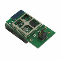
Manufacturer Part Number
EM357-MOD-LR-ANT-TG
Description
MODULE EM357 PA/LNA W/ANT TG
Manufacturer
Ember
Specifications of EM357-MOD-LR-ANT-TG
Frequency
2.4GHz
Data Rate - Maximum
250kbps
Modulation Or Protocol
802.15.4 Zigbee
Voltage - Supply
2.1 V ~ 3.6 V
Current - Receiving
25mA
Current - Transmitting
42mA
Data Interface
PCB, Surface Mount
Memory Size
192kB Flash, 12kB RAM
Antenna Connector
On-Board, Chip
Operating Temperature
-40°C ~ 85°C
Package / Case
Module
Lead Free Status / RoHS Status
Lead free / RoHS Compliant
Power - Output
-
Applications
-
Sensitivity
-
Other names
636-1020


19 Mechanical Details
19.1 QFN48 Footprint Recommendations
The EM35x package is a plastic 48-pin QFN that is 7 mm x 7 mm x 0.90 mm. Figure 19-1 illustrates the package
drawing.
Figure 19-2 demonstrates the IPC-7351 recommended PCB Footprint for the EM35x (QFN50P700X700X90-49N).
A ground pad in the bottom center of the package forms a 49
A 3 x 3 array of non-thermal vias should connect the EM35x decal center shown in Figure 19-2 to the PCB
ground plane through the ground pad. In order to properly solder the EM35x to the footprint, the Paste Mask
layer should have a 3 x 3 array of circular openings at 1.015 mm diameter spaced approximately 1.625 mm
(center to center) apart, as shown in Figure 19-3. This will cause an evenly distributed solder flow and
coplanar attachment to the PCB. The solder mask layer (illustrated in Figure 19-4) should be the same as the
copper layer for the EM35x footprint.
For more information on the package footprint, please refer to the appropriate EM35x Reference Design.
Figure 19-1. Package Drawing
Final
19-1
th
pin.
EM351 / EM357
120-035X-000G
Related parts for EM357-MOD-LR-ANT-TG
Image
Part Number
Description
Manufacturer
Datasheet
Request
R

Part Number:
Description:
MODULE EM357 NO PA/LNA W/ANT TG
Manufacturer:
Ember
Datasheet:

Part Number:
Description:
MODULE EM357 NO PA/LNA W/RF CONN
Manufacturer:
Ember
Datasheet:
Part Number:
Description:
MODULE EM357 PA/LNA W/RF CONN
Manufacturer:
Ember
Datasheet:

Part Number:
Description:
KIT DEV EMBER ZIGBEE W/PCWH
Manufacturer:
Custom Computer Services Inc (CCS)

Part Number:
Description:
PROGRAMMER USB FLASH EM250/260
Manufacturer:
Ember
Datasheet:

Part Number:
Description:
IC ZIGBEE SYSTEM-ON-CHIP 40-QFN
Manufacturer:
Ember
Datasheet:

Part Number:
Description:
IC ZIGBEE SYSTEM-ON-CHIP 48-QFN
Manufacturer:
Ember
Datasheet:
Part Number:
Description:
IC RF TXRX ZIGBEE 128KB 48QFN
Manufacturer:
Ember
Datasheet:
Part Number:
Description:
IC RF TXRX ZIGBEE 192KB 48QFN
Manufacturer:
Ember
Datasheet:

Part Number:
Description:
INSIGHT ADAPTER FOR EM2XX
Manufacturer:
Ember
Datasheet:

Part Number:
Description:
IAR EWARM LICENCE FOR EM35X
Manufacturer:
Ember
Datasheet:

Part Number:
Description:
KIT EVAL EM250 RF TEST
Manufacturer:
Ember
Datasheet:

Part Number:
Description:
INSIGHT ADAPTER 3 FOR EM35X
Manufacturer:
Ember
Datasheet:

Part Number:
Description:
EM250 RCM BOARD
Manufacturer:
Ember
Datasheet:

Part Number:
Description:
EM35X BREAKOUT BOARD
Manufacturer:
Ember
Datasheet: