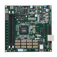
LFE3-95E-PCIE-DKN Lattice, LFE3-95E-PCIE-DKN Datasheet - Page 108

LFE3-95E-PCIE-DKN
Manufacturer Part Number
LFE3-95E-PCIE-DKN
Description
MCU, MPU & DSP Development Tools LatticeECP3 PCI Express Dev Kit
Manufacturer
Lattice
Datasheet
1.LFE3-150EA-7FN672CTW.pdf
(130 pages)
Specifications of LFE3-95E-PCIE-DKN
Processor To Be Evaluated
LFE3-95EA-x
Processor Series
LatticeECP3
Interface Type
SPI
Operating Supply Voltage
1.2 V to 3.3 V
Lead Free Status / RoHS Status
Lead free / RoHS Compliant
- Current page: 108 of 130
- Download datasheet (3Mb)
Z
R
V
V
V
V
V
V
T
T
Note: Data is for 6mA differential current drive. Other differential driver current options are available.
Lattice Semiconductor
sysI/O Differential Electrical Characteristics
Transition Reduced LVDS (TRLVDS DC Specification)
Mini LVDS
Parameter Symbol
O
R
ODUTY
OD
OS
THD
CM
T
OD
, T
ID
F
V
V
V
V
R
Note: LatticeECP3 only supports the TRLVDS receiver.
CCO
ID
ICM
CCO
T
Symbol
Driver supply voltage (+/- 5%)
Input differential voltage
Input common mode voltage
Termination supply voltage
Termination resistance (off-chip)
Single-ended PCB trace impedance
Differential termination resistance
Output voltage, differential, |V
Output voltage, common mode, |V
Change in V
Change in V
Input voltage, differential, |V
Input voltage, common mode, |V
Output rise and fall times, 20% to 80%
Output clock duty cycle
Current
Source
Description
Transmitter
OD
OS
Over Recommended Operating Conditions
Over Recommended Operating Conditions
, between H and L
, between H and L
Description
INP
OP
- V
INP
- V
OP
INM
OM
+ V
+ V
|
3-56
|
INM
OM
Z
Min.
3.14
3.14
0
150
45
|/2 0.3+(V
|/2
3
Min.
300
200
30
50
40
—
—
—
1
THD
DC and Switching Characteristics
Nom.
R
/2)
3.3
3.3
50
T
LatticeECP3 Family Data Sheet
VCCO = 3.3V
R
T
Receiver
Typ.
100
1.2
50
—
—
—
—
—
—
—
3.265
Max.
1200
3.47
3.47
55
2.1-(V
Max.
150
600
600
550
1.4
75
60
50
50
THD
/2)
Ohms
Units
mV
V
V
V
Units
ohms
ohms
mV
mV
mV
mV
ps
%
V
Related parts for LFE3-95E-PCIE-DKN
Image
Part Number
Description
Manufacturer
Datasheet
Request
R

Part Number:
Description:
FPGA - Field Programmable Gate Array 92K LUTs, 490 I/O 8 Speed
Manufacturer:
Lattice

Part Number:
Description:
FPGA - Field Programmable Gate Array 92K LUTs, 380 I/O 7 Speed
Manufacturer:
Lattice

Part Number:
Description:
FPGA - Field Programmable Gate Array 92K LUTs, 295 I/O 7 Speed
Manufacturer:
Lattice

Part Number:
Description:
FPGA - Field Programmable Gate Array 92K LUTs, 380 I/O 6 Speed
Manufacturer:
Lattice

Part Number:
Description:
FPGA - Field Programmable Gate Array 92K LUTs, 490 I/O 6 Speed
Manufacturer:
Lattice

Part Number:
Description:
FPGA - Field Programmable Gate Array 92K LUTs, 295 I/O 8 Speed
Manufacturer:
Lattice

Part Number:
Description:
FPGA - Field Programmable Gate Array 92K LUTs, 490 I/O 8 Speed
Manufacturer:
Lattice

Part Number:
Description:
FPGA - Field Programmable Gate Array 92K LUTs, 380 I/O 8 Speed
Manufacturer:
Lattice

Part Number:
Description:
FPGA - Field Programmable Gate Array 92K LUTs, 490 I/O 6 Speed
Manufacturer:
Lattice

Part Number:
Description:
FPGA - Field Programmable Gate Array 92K LUTs, 295 I/O 6 Speed
Manufacturer:
Lattice

Part Number:
Description:
FPGA - Field Programmable Gate Array 92K LUTs, 490 I/O 7 Speed
Manufacturer:
Lattice

Part Number:
Description:
FPGA - Field Programmable Gate Array 92K LUTs, 295 I/O 8 Speed
Manufacturer:
Lattice

Part Number:
Description:
FPGA - Field Programmable Gate Array 92K LUTs, 490 I/O 7 Speed
Manufacturer:
Lattice

Part Number:
Description:
FPGA - Field Programmable Gate Array 92K LUTs, 380 I/O 6 Speed
Manufacturer:
Lattice

Part Number:
Description:
FPGA - Field Programmable Gate Array 92K LUTs, 295 I/O 7 Speed
Manufacturer:
Lattice


