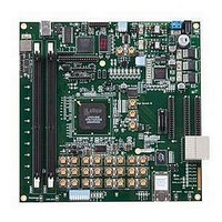
LFE3-95E-PCIE-DKN Lattice, LFE3-95E-PCIE-DKN Datasheet - Page 51

LFE3-95E-PCIE-DKN
Manufacturer Part Number
LFE3-95E-PCIE-DKN
Description
MCU, MPU & DSP Development Tools LatticeECP3 PCI Express Dev Kit
Manufacturer
Lattice
Datasheet
1.LFE3-150EA-7FN672CTW.pdf
(130 pages)
Specifications of LFE3-95E-PCIE-DKN
Processor To Be Evaluated
LFE3-95EA-x
Processor Series
LatticeECP3
Interface Type
SPI
Operating Supply Voltage
1.2 V to 3.3 V
Lead Free Status / RoHS Status
Lead free / RoHS Compliant
Lattice Semiconductor
access port consists of dedicated I/Os: TDI, TDO, TCK and TMS. The test access port has its own supply voltage
V
For more information, please see TN1169,
Device Configuration
All LatticeECP3 devices contain two ports that can be used for device configuration. The Test Access Port (TAP),
which supports bit-wide configuration, and the sysCONFIG port, support dual-byte, byte and serial configuration.
The TAP supports both the IEEE Standard 1149.1 Boundary Scan specification and the IEEE Standard 1532 In-
System Configuration specification. The sysCONFIG port includes seven I/Os used as dedicated pins with the
remaining pins used as dual-use pins. See TN1169,
about using the dual-use pins as general purpose I/Os.
There are various ways to configure a LatticeECP3 device:
1. JTAG
2. Standard Serial Peripheral Interface (SPI and SPIm modes) - interface to boot PROM memory
3. System microprocessor to drive a x8 CPU port (PCM mode)
4. System microprocessor to drive a serial slave SPI port (SSPI mode)
5. Generic byte wide flash with a MachXO™ device, providing control and addressing
On power-up, the FPGA SRAM is ready to be configured using the selected sysCONFIG port. Once a configuration
port is selected, it will remain active throughout that configuration cycle. The IEEE 1149.1 port can be activated any
time after power-up by sending the appropriate command through the TAP port.
LatticeECP3 devices also support the Slave SPI Interface. In this mode, the FPGA behaves like a SPI Flash device
(slave mode) with the SPI port of the FPGA to perform read-write operations.
Enhanced Configuration Options
LatticeECP3 devices have enhanced configuration features such as: decryption support, TransFR™ I/O and dual-
boot image support.
1. TransFR (Transparent Field Reconfiguration)
2. Dual-Boot Image Support
Soft Error Detect (SED) Support
LatticeECP3 devices have dedicated logic to perform Cycle Redundancy Code (CRC) checks. During configura-
tion, the configuration data bitstream can be checked with the CRC logic block. In addition, the LatticeECP3 device
CCJ
TransFR I/O (TFR) is a unique Lattice technology that allows users to update their logic in the field without
interrupting system operation using a single ispVM command. TransFR I/O allows I/O states to be frozen dur-
ing device configuration. This allows the device to be field updated with a minimum of system disruption and
downtime. See TN1087,
details.
Dual-boot images are supported for applications requiring reliable remote updates of configuration data for the
system FPGA. After the system is running with a basic configuration, a new boot image can be downloaded
remotely and stored in a separate location in the configuration storage device. Any time after the update the
LatticeECP3 can be re-booted from this new configuration file. If there is a problem, such as corrupt data dur-
ing download or incorrect version number with this new boot image, the LatticeECP3 device can revert back to
the original backup golden configuration and try again. This all can be done without power cycling the system.
For more information, please see TN1169,
and can operate with LVCMOS3.3, 2.5, 1.8, 1.5 and 1.2 standards.
Minimizing System Interruption During Configuration Using TransFR Technology
LatticeECP3 sysCONFIG Usage
LatticeECP3 sysCONFIG Usage
LatticeECP3 sysCONFIG Usage Guide
2-48
LatticeECP3 Family Data Sheet
Guide.
Guide.
for more information
Architecture
for


