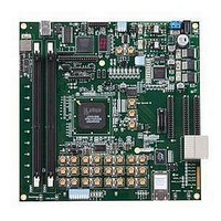
LFE3-95E-PCIE-DKN Lattice, LFE3-95E-PCIE-DKN Datasheet - Page 22

LFE3-95E-PCIE-DKN
Manufacturer Part Number
LFE3-95E-PCIE-DKN
Description
MCU, MPU & DSP Development Tools LatticeECP3 PCI Express Dev Kit
Manufacturer
Lattice
Datasheet
1.LFE3-150EA-7FN672CTW.pdf
(130 pages)
Specifications of LFE3-95E-PCIE-DKN
Processor To Be Evaluated
LFE3-95EA-x
Processor Series
LatticeECP3
Interface Type
SPI
Operating Supply Voltage
1.2 V to 3.3 V
Lead Free Status / RoHS Status
Lead free / RoHS Compliant
- Current page: 22 of 130
- Download datasheet (3Mb)
Lattice Semiconductor
The edge clocks on the top, left, and right sides of the device can drive the secondary clocks or general routing
resources of the device. The left and right side edge clocks also can drive the primary clock network through the
clock dividers (CLKDIV).
sysMEM Memory
LatticeECP3 devices contain a number of sysMEM Embedded Block RAM (EBR). The EBR consists of an 18-Kbit
RAM with memory core, dedicated input registers and output registers with separate clock and clock enable. Each
EBR includes functionality to support true dual-port, pseudo dual-port, single-port RAM, ROM and FIFO buffers
(via external PFUs).
sysMEM Memory Block
The sysMEM block can implement single port, dual port or pseudo dual port memories. Each block can be used in
a variety of depths and widths as shown in Table 2-7. FIFOs can be implemented in sysMEM EBR blocks by imple-
menting support logic with PFUs. The EBR block facilitates parity checking by supporting an optional parity bit for
each data byte. EBR blocks provide byte-enable support for configurations with18-bit and 36-bit data widths. For
more information, please see TN1179,
Table 2-7. sysMEM Block Configurations
Bus Size Matching
All of the multi-port memory modes support different widths on each of the ports. The RAM bits are mapped LSB
word 0 to MSB word 0, LSB word 1 to MSB word 1, and so on. Although the word size and number of words for
each port varies, this mapping scheme applies to each port.
RAM Initialization and ROM Operation
If desired, the contents of the RAM can be pre-loaded during device configuration. By preloading the RAM block
during the chip configuration cycle and disabling the write controls, the sysMEM block can also be utilized as a
ROM.
Memory Cascading
Larger and deeper blocks of RAM can be created using EBR sysMEM Blocks. Typically, the Lattice design tools
cascade memory transparently, based on specific design inputs.
Single Port
True Dual Port
Pseudo Dual Port
Memory Mode
LatticeECP3 Memory Usage
2-19
Configurations
16,384 x 1
1,024 x 18
16,384 x 1
1,024 x 18
16,384 x 1
1,024 x 18
8,192 x 2
4,096 x 4
2,048 x 9
8,192 x 2
4,096 x 4
2,048 x 9
8,192 x 2
4,096 x 4
2,048 x 9
512 x 36
512 x 36
Guide.
LatticeECP3 Family Data Sheet
Architecture
Related parts for LFE3-95E-PCIE-DKN
Image
Part Number
Description
Manufacturer
Datasheet
Request
R

Part Number:
Description:
FPGA - Field Programmable Gate Array 92K LUTs, 490 I/O 8 Speed
Manufacturer:
Lattice

Part Number:
Description:
FPGA - Field Programmable Gate Array 92K LUTs, 380 I/O 7 Speed
Manufacturer:
Lattice

Part Number:
Description:
FPGA - Field Programmable Gate Array 92K LUTs, 295 I/O 7 Speed
Manufacturer:
Lattice

Part Number:
Description:
FPGA - Field Programmable Gate Array 92K LUTs, 380 I/O 6 Speed
Manufacturer:
Lattice

Part Number:
Description:
FPGA - Field Programmable Gate Array 92K LUTs, 490 I/O 6 Speed
Manufacturer:
Lattice

Part Number:
Description:
FPGA - Field Programmable Gate Array 92K LUTs, 295 I/O 8 Speed
Manufacturer:
Lattice

Part Number:
Description:
FPGA - Field Programmable Gate Array 92K LUTs, 490 I/O 8 Speed
Manufacturer:
Lattice

Part Number:
Description:
FPGA - Field Programmable Gate Array 92K LUTs, 380 I/O 8 Speed
Manufacturer:
Lattice

Part Number:
Description:
FPGA - Field Programmable Gate Array 92K LUTs, 490 I/O 6 Speed
Manufacturer:
Lattice

Part Number:
Description:
FPGA - Field Programmable Gate Array 92K LUTs, 295 I/O 6 Speed
Manufacturer:
Lattice

Part Number:
Description:
FPGA - Field Programmable Gate Array 92K LUTs, 490 I/O 7 Speed
Manufacturer:
Lattice

Part Number:
Description:
FPGA - Field Programmable Gate Array 92K LUTs, 295 I/O 8 Speed
Manufacturer:
Lattice

Part Number:
Description:
FPGA - Field Programmable Gate Array 92K LUTs, 490 I/O 7 Speed
Manufacturer:
Lattice

Part Number:
Description:
FPGA - Field Programmable Gate Array 92K LUTs, 380 I/O 6 Speed
Manufacturer:
Lattice

Part Number:
Description:
FPGA - Field Programmable Gate Array 92K LUTs, 295 I/O 7 Speed
Manufacturer:
Lattice


