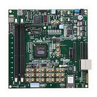
LFE3-95E-PCIE-DKN Lattice, LFE3-95E-PCIE-DKN Datasheet - Page 93

LFE3-95E-PCIE-DKN
Manufacturer Part Number
LFE3-95E-PCIE-DKN
Description
MCU, MPU & DSP Development Tools LatticeECP3 PCI Express Dev Kit
Manufacturer
Lattice
Datasheet
1.LFE3-150EA-7FN672CTW.pdf
(130 pages)
Specifications of LFE3-95E-PCIE-DKN
Processor To Be Evaluated
LFE3-95EA-x
Processor Series
LatticeECP3
Interface Type
SPI
Operating Supply Voltage
1.2 V to 3.3 V
Lead Free Status / RoHS Status
Lead free / RoHS Compliant
- Current page: 93 of 130
- Download datasheet (3Mb)
Lattice Semiconductor
XAUI/Serial Rapid I/O Type 3 Electrical and Timing Characteristics
AC and DC Characteristics
Table 3-13. Transmit
Table 3-14. Receive and Jitter Tolerance
T
Z
J
J
1. Total jitter includes both deterministic jitter and random jitter.
2. Jitter values are measured with each CML output AC coupled into a 50-ohm impedance (100-ohm differential impedance).
3. Jitter and skew are specified between differential crossings of the 50% threshold of the reference signal.
4. Values are measured at 2.5 Gbps.
RL
RL
Z
J
J
J
J
T
1. Total jitter includes deterministic jitter, random jitter and sinusoidal jitter. The sinusoidal jitter tolerance mask is shown in Figure 3-14.
2. Jitter values are measured with each high-speed input AC coupled into a 50-ohm impedance.
3. Jitter and skew are specified between differential crossings of the 50% threshold of the reference signal.
4. Jitter tolerance parameters are characterized when Full Rx Equalization is enabled.
5. Values are measured at 2.5 Gbps.
TX_DDJ
TX_TJ
RX_DJ
RX_RJ
RX_SJ
RX_TJ
RF
TX_DIFF_DC
RX_DIFF
RX_EYE
RX_DIFF
RX_CM
Symbol
Symbol
1, 2, 3, 4
1, 2, 3
1, 2, 3
1, 2, 3
1, 2, 3
2, 3, 4
Differential return loss
Common mode return loss
Differential termination resistance
Deterministic jitter tolerance (peak-to-peak)
Random jitter tolerance (peak-to-peak)
Sinusoidal jitter tolerance (peak-to-peak)
Total jitter tolerance (peak-to-peak)
Receiver eye opening
Differential rise/fall time
Differential impedance
Output data deterministic jitter
Total output data jitter
Description
Description
Over Recommended Operating Conditions
Over Recommended Operating Conditions
3-41
Test Conditions
From 100 MHz
to 3.125 GHz
From 100 MHz
to 3.125 GHz
Test Conditions
20%-80%
DC and Switching Characteristics
LatticeECP3 Family Data Sheet
Min.
80
—
—
—
Min.
0.35
10
80
—
—
—
—
6
Typ.
100
80
—
—
Typ.
100
—
—
—
—
—
—
—
Max.
0.17
0.35
120
—
Max.
0.37
0.18
0.10
0.65
120
—
—
—
Ohms
Units
Ohms
Units
ps
UI
UI
dB
dB
UI
UI
UI
UI
UI
Related parts for LFE3-95E-PCIE-DKN
Image
Part Number
Description
Manufacturer
Datasheet
Request
R

Part Number:
Description:
FPGA - Field Programmable Gate Array 92K LUTs, 490 I/O 8 Speed
Manufacturer:
Lattice

Part Number:
Description:
FPGA - Field Programmable Gate Array 92K LUTs, 380 I/O 7 Speed
Manufacturer:
Lattice

Part Number:
Description:
FPGA - Field Programmable Gate Array 92K LUTs, 295 I/O 7 Speed
Manufacturer:
Lattice

Part Number:
Description:
FPGA - Field Programmable Gate Array 92K LUTs, 380 I/O 6 Speed
Manufacturer:
Lattice

Part Number:
Description:
FPGA - Field Programmable Gate Array 92K LUTs, 490 I/O 6 Speed
Manufacturer:
Lattice

Part Number:
Description:
FPGA - Field Programmable Gate Array 92K LUTs, 295 I/O 8 Speed
Manufacturer:
Lattice

Part Number:
Description:
FPGA - Field Programmable Gate Array 92K LUTs, 490 I/O 8 Speed
Manufacturer:
Lattice

Part Number:
Description:
FPGA - Field Programmable Gate Array 92K LUTs, 380 I/O 8 Speed
Manufacturer:
Lattice

Part Number:
Description:
FPGA - Field Programmable Gate Array 92K LUTs, 490 I/O 6 Speed
Manufacturer:
Lattice

Part Number:
Description:
FPGA - Field Programmable Gate Array 92K LUTs, 295 I/O 6 Speed
Manufacturer:
Lattice

Part Number:
Description:
FPGA - Field Programmable Gate Array 92K LUTs, 490 I/O 7 Speed
Manufacturer:
Lattice

Part Number:
Description:
FPGA - Field Programmable Gate Array 92K LUTs, 295 I/O 8 Speed
Manufacturer:
Lattice

Part Number:
Description:
FPGA - Field Programmable Gate Array 92K LUTs, 490 I/O 7 Speed
Manufacturer:
Lattice

Part Number:
Description:
FPGA - Field Programmable Gate Array 92K LUTs, 380 I/O 6 Speed
Manufacturer:
Lattice

Part Number:
Description:
FPGA - Field Programmable Gate Array 92K LUTs, 295 I/O 7 Speed
Manufacturer:
Lattice


