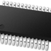
PIC24FJ64GB002-I/SS Microchip Technology, PIC24FJ64GB002-I/SS Datasheet - Page 194

PIC24FJ64GB002-I/SS
Manufacturer Part Number
PIC24FJ64GB002-I/SS
Description
16-bit, 16 MIPS, 64KB Flash, 8KB RAM, Nanowatt XLP, USB OTG 28 SSOP .209in TUBE
Manufacturer
Microchip Technology
Specifications of PIC24FJ64GB002-I/SS
Processor Series
PIC24
Core
PIC24F
Data Bus Width
16 bit
Program Memory Type
Flash
Program Memory Size
64 KB
Data Ram Size
8192 B
Interface Type
I2C, SPI, UART
Maximum Clock Frequency
32 MHz
Number Of Programmable I/os
21
Number Of Timers
5
Operating Supply Voltage
2 V to 3.6 V
Maximum Operating Temperature
+ 85 C
Mounting Style
SMD/SMT
Package / Case
SSOP-28
Development Tools By Supplier
MPLAB Integrated Development Environment
Minimum Operating Temperature
- 40 C
Operating Temperature Range
- 40 C to + 85 C
Supply Current (max)
300 mA
Lead Free Status / Rohs Status
Lead free / RoHS Compliant
Available stocks
Company
Part Number
Manufacturer
Quantity
Price
Part Number:
PIC24FJ64GB002-I/SS
Manufacturer:
MICROCHIP/微芯
Quantity:
20 000
- Current page: 194 of 352
- Download datasheet (3Mb)
PIC24FJ64GB004 FAMILY
REGISTER 17-2:
DS39940D-page 194
bit 15
bit 7
Legend:
R = Readable bit
-n = Value at POR
bit 15,13
bit 14
bit 12
bit 11
bit 10
bit 9
bit 8
bit 7-6
Note 1:
URXISEL1
UTXISEL1
R/W-0
R/W-0
2:
Value of bit only affects the transmit properties of the module when the IrDA encoder is enabled (IREN = 1).
If UARTEN = 1, the peripheral inputs and outputs must be configured to an available RPn pin. See
Section 10.4 “Peripheral Pin Select (PPS)” for more information.
UTXISEL<1:0>: Transmission Interrupt Mode Selection bits
11 = Reserved; do not use
10 = Interrupt when a character is transferred to the Transmit Shift Register (TSR), and as a result,
01 = Interrupt when the last character is shifted out of the Transmit Shift Register; all transmit
00 = Interrupt when a character is transferred to the Transmit Shift Register (this implies there is at
UTXINV: IrDA
IREN = 0:
1 = UxTX Idle ‘0’
0 = UxTX Idle ‘1’
IREN = 1:
1 = UxTX Idle ‘1’
0 = UxTX Idle ‘0’
Unimplemented: Read as ‘0’
UTXBRK: Transmit Break bit
1 = Send Sync Break on next transmission – Start bit, followed by twelve ‘0’ bits, followed by Stop bit;
0 = Sync Break transmission disabled or completed
UTXEN: Transmit Enable bit
1 = Transmit enabled, UxTX pin controlled by UARTx
0 = Transmit disabled, any pending transmission is aborted and the buffer is reset; UxTX pin controlled
UTXBF: Transmit Buffer Full Status bit (read-only)
1 = Transmit buffer is full
0 = Transmit buffer is not full; at least one more character can be written
TRMT: Transmit Shift Register Empty bit (read-only)
1 = Transmit Shift Register is empty and transmit buffer is empty (the last transmission has completed)
0 = Transmit Shift Register is not empty, a transmission is in progress or queued
URXISEL<1:0>: Receive Interrupt Mode Selection bits
11 = Interrupt is set on RSR transfer, making the receive buffer full (i.e., has 4 data characters)
10 = Interrupt is set on RSR transfer, making the receive buffer 3/4 full (i.e., has 3 data characters)
0x = Interrupt is set when any character is received and transferred from the RSR to the receive buffer;
URXISEL0
UTXINV
R/W-0
R/W-0
cleared by hardware upon completion
by port
the transmit buffer becomes empty
operations are completed
least one character open in the transmit buffer)
receive buffer has one or more characters
UxSTA: UARTx STATUS AND CONTROL REGISTER
(1)
®
C = Clearable bit
W = Writable bit
‘1’ = Bit is set
UTXISEL0
Encoder Transmit Polarity Inversion bit
ADDEN
R/W-0
R/W-0
(2)
RIDLE
U-0
R-1
—
HC = Hardware Clearable bit
U = Unimplemented bit, read as ‘0’
‘0’ = Bit is cleared
R/W-0, HC
UTXBRK
PERR
R-0
(1)
UTXEN
R/W-0
FERR
R-0
(2)
2010 Microchip Technology Inc.
x = Bit is unknown
UTXBF
OERR
R/C-0
R-0
URXDA
TRMT
R-1
R-0
bit 8
bit 0
Related parts for PIC24FJ64GB002-I/SS
Image
Part Number
Description
Manufacturer
Datasheet
Request
R

Part Number:
Description:
Manufacturer:
Microchip Technology Inc.
Datasheet:

Part Number:
Description:
Manufacturer:
Microchip Technology Inc.
Datasheet:

Part Number:
Description:
Manufacturer:
Microchip Technology Inc.
Datasheet:

Part Number:
Description:
Manufacturer:
Microchip Technology Inc.
Datasheet:

Part Number:
Description:
Manufacturer:
Microchip Technology Inc.
Datasheet:

Part Number:
Description:
Manufacturer:
Microchip Technology Inc.
Datasheet:

Part Number:
Description:
Manufacturer:
Microchip Technology Inc.
Datasheet:

Part Number:
Description:
Manufacturer:
Microchip Technology Inc.
Datasheet:


