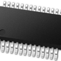
PIC24FJ64GB002-I/SS Microchip Technology, PIC24FJ64GB002-I/SS Datasheet - Page 221

PIC24FJ64GB002-I/SS
Manufacturer Part Number
PIC24FJ64GB002-I/SS
Description
16-bit, 16 MIPS, 64KB Flash, 8KB RAM, Nanowatt XLP, USB OTG 28 SSOP .209in TUBE
Manufacturer
Microchip Technology
Specifications of PIC24FJ64GB002-I/SS
Processor Series
PIC24
Core
PIC24F
Data Bus Width
16 bit
Program Memory Type
Flash
Program Memory Size
64 KB
Data Ram Size
8192 B
Interface Type
I2C, SPI, UART
Maximum Clock Frequency
32 MHz
Number Of Programmable I/os
21
Number Of Timers
5
Operating Supply Voltage
2 V to 3.6 V
Maximum Operating Temperature
+ 85 C
Mounting Style
SMD/SMT
Package / Case
SSOP-28
Development Tools By Supplier
MPLAB Integrated Development Environment
Minimum Operating Temperature
- 40 C
Operating Temperature Range
- 40 C to + 85 C
Supply Current (max)
300 mA
Lead Free Status / Rohs Status
Lead free / RoHS Compliant
Available stocks
Company
Part Number
Manufacturer
Quantity
Price
Part Number:
PIC24FJ64GB002-I/SS
Manufacturer:
MICROCHIP/微芯
Quantity:
20 000
- Current page: 221 of 352
- Download datasheet (3Mb)
REGISTER 18-12: U1CNFG1: USB CONFIGURATION REGISTER 1 (CONTINUED)
REGISTER 18-13: U1CNFG2: USB CONFIGURATION REGISTER 2
2010 Microchip Technology Inc.
bit 1-0
Note 1:
bit 15
bit 7
Legend:
R = Readable bit
-n = Value at POR
bit 15-6
bit 5
bit 4
bit 3
bit 2
bit 1
bit 0
Note 1:
U-0
U-0
—
—
This bit is only active when the UTRDIS bit (U1CNFG2<0>) is set.
Never change these bits while the USBPWR bit is set (U1PWRC<0> = 1).
PPB<1:0>: Ping-Pong Buffers Configuration bit
11 = EVEN/ODD ping-pong buffers are enabled for Endpoints 1 to 15
10 = EVEN/ODD ping-pong buffers are enabled for all endpoints
01 = EVEN/ODD ping-pong buffers are enabled for OUT Endpoint 0
00 = EVEN/ODD ping-pong are buffers are disabled
Unimplemented: Read as ‘0’
UVCMPSEL: External Comparator Input Mode Select bit (see Table 18-3)
When UVCMPDIS is set:
1 = Use 3 pin input for external comparators
0 = Use 2 pin input for external comparators
PUVBUS: V
1 = Pull-up on V
0 = Pull-up on V
EXTI2CEN: I
1 = External module(s) is controlled via I
0 = External module(s) is controlled via dedicated pins
UVBUSDIS: On-Chip 5V Boost Regulator Builder Disable bit
1 = On-chip boost regulator builder is disabled; digital output control interface is enabled
0 = On-chip boost regulator builder is active
UVCMPDIS: On-Chip V
1 = On-chip charge V
0 = On-chip charge V
UTRDIS: On-Chip Transceiver Disable bit
1 = On-chip transceiver is disabled; digital transceiver interface is enabled
0 = On-chip transceiver is active
U-0
U-0
—
—
BUS
2
C™ Interface For External Module Control Enable bit
W = Writable bit
‘1’ = Bit is set
UVCMPSEL
Pull-up Enable bit
BUS
BUS
R/W-0
U-0
—
pin is enabled
pin is disabled
BUS
BUS
BUS
comparator is disabled; digital input status interface is enabled
comparator is active
Comparator Disable bit
PUVBUS
R/W-0
U-0
PIC24FJ64GB004 FAMILY
—
2
(1)
C interface
U = Unimplemented bit, read as ‘0’
‘0’ = Bit is cleared
EXTI2CEN
R/W-0
U-0
—
(1)
UVBUSDIS
(1)
R/W-0
U-0
—
(1)
UVCMPDIS
x = Bit is unknown
R/W-0
U-0
—
DS39940D-page 221
(1)
UTRDIS
R/W-0
U-0
—
bit 8
bit 0
(1)
Related parts for PIC24FJ64GB002-I/SS
Image
Part Number
Description
Manufacturer
Datasheet
Request
R

Part Number:
Description:
Manufacturer:
Microchip Technology Inc.
Datasheet:

Part Number:
Description:
Manufacturer:
Microchip Technology Inc.
Datasheet:

Part Number:
Description:
Manufacturer:
Microchip Technology Inc.
Datasheet:

Part Number:
Description:
Manufacturer:
Microchip Technology Inc.
Datasheet:

Part Number:
Description:
Manufacturer:
Microchip Technology Inc.
Datasheet:

Part Number:
Description:
Manufacturer:
Microchip Technology Inc.
Datasheet:

Part Number:
Description:
Manufacturer:
Microchip Technology Inc.
Datasheet:

Part Number:
Description:
Manufacturer:
Microchip Technology Inc.
Datasheet:


