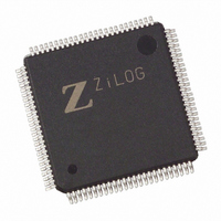
Z8018233ASG Zilog, Z8018233ASG Datasheet - Page 11

Z8018233ASG
Manufacturer Part Number
Z8018233ASG
Description
IC 33MHZ STATIC MIMIC 100-LQFP
Manufacturer
Zilog
Datasheet
1.Z8018233FSG.pdf
(109 pages)
Specifications of Z8018233ASG
Processor Type
Z180
Features
Smart Peripheral Controller
Speed
33MHz
Voltage
5V
Mounting Type
Surface Mount
Package / Case
100-LQFP
Processor Series
Z8018xx
Core
Z80
Data Bus Width
8 bit
Program Memory Type
ROMLess
Interface Type
UART
Maximum Clock Frequency
33 MHz
Number Of Programmable I/os
24
Number Of Timers
2
Operating Supply Voltage
4.5 V to 5.5 V
Maximum Operating Temperature
+ 70 C
Mounting Style
SMD/SMT
Minimum Operating Temperature
0 C
Lead Free Status / RoHS Status
Lead free / RoHS Compliant
Available stocks
Company
Part Number
Manufacturer
Quantity
Price
MULTIPLEXED PIN DESCRIPTIONS
A18/T
If either TOC1 or TOC0 bit of the Timer Control Register
(TCR) is set to 1, The T
TOC0 bits are cleared to 0, the A18 function is selected.
In normal user mode (on-chip bus master), the A18 signal
for the chip select logic is obtained from the CPU before
the external pin is muxed as A18/T
selection of T
select logic. However, in adapter mode (off-chip bus
master), the A18 signal MUST be provided by the external
bus master.
CKA0//DREQ0. During Reset, this pin is initialized as
CKA0 pin. If either DM1 or SM1 in the DMA Mode Register
(DMODE) is set to 1, /DREQ0 function is always selected.
CKA1//TEND0. During Reset, this pin is initialized as
CKA1 pin. If CKA1D bit in the ASCI control register
Ch1(CNTLA1) is set to 1, /TEND0 function is selected. If
CKA1D bit is set to 0, CKA1 function is selected.
RxS//CTS1. During Reset, this pin is initialized as the RxS
pin. If CTS1E bit in the ASCI status register Ch1 (STAT1) is
set to 1, /CTS1 function is selected. If CTS1E bit is set to 0,
RxS function is selected. This pin is also multiplexed with
PB7 based on bit 6 in the System Configuration Register.
The pins below are triple-multiplexed based upon the
values of bit 1 and bit 2 of the System Configuration
Register. The pins are configured as Table 2 specifies. On
Reset, both bits 1 and 2 are 0, so /TEND1,TxS,CKS are
selected.
DS971820600
Zilog
OUT.
During Reset, this pin is initialized as an A18 pin.
OUT
will not affect the operation of the 182 chip
OUT
function is selected. If TOC1 and
OUT
. Therefore, the
PS009801-0301
P R E L I M I N A R Y
The pins below are multiplexed based upon the value of bit
1 of the System Configuration register. If bit 1 is 0, then the
Z80182/Z8L182 Mode 0 (non-16550 MIMIC mode) signals
are selected; if bit 1 is 1, then Z80182/Z8L182 Mode 1
(16550 MIMIC mode) signals are selected. On Reset,
Z80182/Z8L182 Mode 0 is always selected as shown in
Table 3.
Bit 1
Z80182/Z8L182
0
0
1
1
Table 3. Mode 0 and Mode 1 Multiplexed Pins
Mode 0
TxDB
RxDB
/TRxCB
/RTxCB
/SYNCB
/CTSB
/DCDB
PA7-PA0
Bit 2
Table 2. Triple Multiplexed Pins
0
1
0
1
Master Configuration Register
/TEND1,TxS,CKS
/RTSB,/DTR//REQB,/W//REQB
/TEND1,TxS,CKS
/HRxRDY,//HTxRDY,HINTR
Z80182/Z8L182
Mode 1
/HDDIS
HA1
HA0
HA2
/HCS
/HWR
/HRD
HD7-HD0
Z
ILOG
I
NTELLIGENT
Z80182/Z8L182
P
ERIPHERAL
3-11


