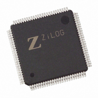
Z8018233ASG Zilog, Z8018233ASG Datasheet - Page 50

Z8018233ASG
Manufacturer Part Number
Z8018233ASG
Description
IC 33MHZ STATIC MIMIC 100-LQFP
Manufacturer
Zilog
Datasheet
1.Z8018233FSG.pdf
(109 pages)
Specifications of Z8018233ASG
Processor Type
Z180
Features
Smart Peripheral Controller
Speed
33MHz
Voltage
5V
Mounting Type
Surface Mount
Package / Case
100-LQFP
Processor Series
Z8018xx
Core
Z80
Data Bus Width
8 bit
Program Memory Type
ROMLess
Interface Type
UART
Maximum Clock Frequency
33 MHz
Number Of Programmable I/os
24
Number Of Timers
2
Operating Supply Voltage
4.5 V to 5.5 V
Maximum Operating Temperature
+ 70 C
Mounting Style
SMD/SMT
Minimum Operating Temperature
0 C
Lead Free Status / RoHS Status
Lead free / RoHS Compliant
Available stocks
Company
Part Number
Manufacturer
Quantity
Price
Zilog
PROGRAMMING THE ESCC
The ESCC contains write registers in each channel that are
programmed by the system separately to configure the
functional uniqueness of the channels.
In the ESCC, the data registers are directly addressed by
selecting a High on the D//C pin. With all other registers
(with the exception of WR0 and RR0), programming the
write registers requires two write operations and reading
the read registers, both a write and a read operation. The
first write is to WR0 and contains three bits that point to the
selected register. The second write is the actual control
word for the selected read register accessed. All of the
ESCC registers, including the data registers, may be
accessed in this fashion. The pointer bits are automatically
cleared after the read or write operation so that WR0 (or
RR0) is addressed again.
With the Z80182/Z8L182, a new feature is implemented in
the ESCC. The Transmitter and Receiver is now capable of
sending and comparing a 32-bit CRC-32 (Ethernet
Polynomial):
x
x
This feature is enabled by access to WR7' Bit 7, which
selects the 32-bit CRC polynomial for the transmitter and
receiver and overrides any selection of SDLC/CRC-16
CRCs. When the 32-bit CRC override feature is enabled,
the transmitter will only send 32-bit CRC when CRC is to be
sent. On the receive side, the CRC comparison/calculation
will be done only on 32-bit CRC values. The result of the
32-bit CRC comparison will be maintained in RR1 bit D6 in
place of the 16-bit CRC comparison result. The 32-bit CRC
compare result will also be maintained in the 10x19 FIFO
for frames in which 32-bit CRC is enabled. The CRC still
can be preset to all 0s or all 1s. 32-bit CRC is disabled upon
power-up or reset.
Note: The ESCC cannot do simultaneous calculation/
comparison using both 16-bit and 32-bit CRC.
Also, for the Z80182/Z8L182 only, the clock provided to the
ESCC core is equal to the system clock divided by 1 or 2.
The divider is programmed in the Z80182 Enhancement
Register bit 3.
3-50
32
2
+ x + 1
+ x
26
+x
23
+x
22
+ x
16
+ x
12
+ x
11
+x
™
10
+ x
8
+ x
P R E L I M I N A R Y
PS009801-0301
7
+ x
5
+ x
4
+
Divide-by-two should be programmed when running the
Z182 beyond:
Note: Upon power-up or reset the system clock is equal to
the ESCC clock.
Initialization. The system program first issues a series of
commands to initialize the basic mode of operation. This
is followed by other commands to qualify conditions within
the selected mode. For example, in the Asynchronous
mode, character length, clock rate, number of stop bits,
and even or odd parity should be set first. Then the
interrupt mode is set, and finally, the receiver and transmitter
are enabled.
Write Registers. The ESCC contains 16 write registers (17
counting the transmit buffer) in each channel. These write
registers are programmed separately to configure the
functional "personality" of the channels. There are two
registers (WR2 and WR9) shared by the two channels that
are accessed through either of them. WR2 contains the
interrupt vector for both channels, while WR9 contains the
interrupt control bits and reset commands. A new register,
WR7', was added to the ESCC and may be written to if
WR15, D0 is set. Figure 50 shows the format of each write
register.
Read Registers. The ESCC contains ten read registers
(eleven, counting the receive buffer (RR8) in each channel).
Four of these may be read to obtain status information
(RR0, RR1, RR10, and RR15). Two registers (RR12 and
RR13) are read to learn the baud rate generator time
constant. RR2 contains either the unmodified interrupt
vector (channel A) or the vector modified by status
information (channel B). RR3 contains the Interrupt Pending
(IP) bits (channel A only). RR6 and RR7 contain the
information in the SDLC Frame Status FIFO, but is only
read when WR15, D2 is set. If WR7' D6 is set, Write
Registers WR3, WR4, WR5, WR7, and WR10 can be read
as RR9, RR4, RR5, and RR14, respectively. Figure 51
shows the format of each Read register.
- 20 MHz, 5V
- 10 MHz, 3V
Z
ILOG
I
NTELLIGENT
DS971820600
Z80182/Z8L182
P
ERIPHERAL


