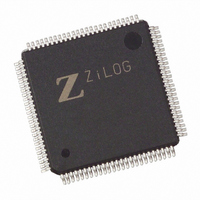
Z8018233ASG Zilog, Z8018233ASG Datasheet - Page 72

Z8018233ASG
Manufacturer Part Number
Z8018233ASG
Description
IC 33MHZ STATIC MIMIC 100-LQFP
Manufacturer
Zilog
Datasheet
1.Z8018233FSG.pdf
(109 pages)
Specifications of Z8018233ASG
Processor Type
Z180
Features
Smart Peripheral Controller
Speed
33MHz
Voltage
5V
Mounting Type
Surface Mount
Package / Case
100-LQFP
Processor Series
Z8018xx
Core
Z80
Data Bus Width
8 bit
Program Memory Type
ROMLess
Interface Type
UART
Maximum Clock Frequency
33 MHz
Number Of Programmable I/os
24
Number Of Timers
2
Operating Supply Voltage
4.5 V to 5.5 V
Maximum Operating Temperature
+ 70 C
Mounting Style
SMD/SMT
Minimum Operating Temperature
0 C
Lead Free Status / RoHS Status
Lead free / RoHS Compliant
Available stocks
Company
Part Number
Manufacturer
Quantity
Price
Zilog
16550 MIMIC REGISTERS (Continued)
Line Status Register
Bit 7 Error in RCVR FIFO
In 16450 mode, this bit will read logic 0. In 16550 mode this
bit is set if at least one data byte is available in the FIFO with
one of its associated error bits set. This bit will clear when
there are no more errors (or break detects) in the FIFO.
Bit 6 Transmitter Empty
This bit must be set or reset by the MPU by a write to this
register bit. If Double Buffer Mode is enabled, the TEMT bit
is set/reset automatically. The function of this bit is modified
when TEMT/Double Buffer enhancement is selected. Refer
to page 3-26 for TEMT/Double Buffer information.
Bit 5 Transmit Holding Register Empty, THRE
This bit is set to 1 when either the THR has been read
(emptied) by the MPU (16450 mode) or the XMIT FIFO is
empty (16550 mode). This bit is set to 0 when either the
THR or XMIT FIFO become non-empty. A shadow bit exists
so that the register bit setting to 1 is delayed by the
Transmitter Timer if enabled. The MPU when reading this
bit will not see the delay. Both shadow and register bits are
cleared when the PC writes to the THR of XMIT FIFO. The
function of this bit is modified when TEMT/Double Buffer
enhancement is selected. Refer to page 3-26 for
TEMT/Double Buffer information.
Bit 2, 3, 4 Parity Error, Framing Error, Break Detect
These bits are written, indirectly, by the MPU as follows:
The bits are first written to shadow bit locations when the
MPU write accesses the LSR. When the next character is
written to the Receive Buffer or RCVR FIFO, the data in the
shadow bits is then copied to the LSR (16450 mode) or
FIFO RAM (16550 mode). In FIFO mode bits become
available to the PC when the data byte associated with the
bits is next to be read (top of FIFO). In FIFO mode, with
successive reads of the receiver, the status bits will be set
if an error occurs on any byte. Once the MPU writes to the
Receive Buffer or RCVR FIFO, the shadow bits are auto
cleared. The register bits are cleared upon the PC reading
the LSR. In FIFO mode these bits will be set if any byte has
the respective error bit set while the PC reads multiple
characters from the FIFO.
Bit 1 Overrun Error
This bit is set if the Z180 MPU makes a second write to the
Receive Buffer before the PC reads the data in the Buffer
(16450 mode) or with a full RCVR FIFO (16550 mode.) No
data will be transferred to the RCVR FIFO under these
circumstances. This bit is reset when the PC reads the Line
Status Register.
3-72
P R E L I M I N A R Y
PS009801-0301
Bit 0 Data Ready
This bit is set to 1 when received data is available, either in
the RCVR FIFO (16550 mode) or Receive Buffer Register
(16450 mode). This bit is set immediately upon the MPU
writing data to the Receive Buffer or FIFO if the Receive
Timer is not enabled but is delayed by the timer interval if
the Receive Timer is enabled. For MPU read access a
shadow bit exists so that the MPU does not see the delay
the PC does. Both bits are cleared to logic zero immediately
upon reading all the data in either the Receive Buffer or
FIFO.
Interrupt Enable Register
Bits 7, 6, 5, 4 Reserved
These bits will always read 0 (PC and MPU).
Bit 3 Modem Status IRQ
If bits 0, 1, 2 or 3 of the Modem Status Register are set and
this enable bit is a logic 1, then an interrupt to the PC is
generated.
Bit 2 Receive Line Status IRQ
If bits 1, 2, 3 or 4 of the LSR are set and this enable bit is
a logic 1, then an interrupt to the PC is generated.
Bit 1 Transmit Holding Register Empty IRQ
If bit 5 of the LSR is set and this enable bit is a logic 1, then
an interrupt to the PC is generated.
Bit 0 Received Data Available IRQ
If bit 0 of the LSR is set or a Receive Timeout occurs and
this enable bit is a logic 1, then an interrupt to the PC is
generated.
D7 D6 D5 D4 D3 D2 D1 D0
0
0
(Z180 MPU Read Only, Address xxF1H)
0
Figure 75. Interrupt Enable Register
0
(PC Read/Write, Address 01H)
0
0
0
0
Bit 0 Received Data Available Int.
Bit 1 THRE Interrupt
Bit 3 MODEM Status Interrupt
Bit 2 Receiver Line Status Int.
Bit 7, 6, 5, 4 Always 0
Z
ILOG
I
NTELLIGENT
DS971820600
Z80182/Z8L182
P
ERIPHERAL


