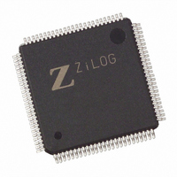
Z8018233ASG Zilog, Z8018233ASG Datasheet - Page 5

Z8018233ASG
Manufacturer Part Number
Z8018233ASG
Description
IC 33MHZ STATIC MIMIC 100-LQFP
Manufacturer
Zilog
Datasheet
1.Z8018233FSG.pdf
(109 pages)
Specifications of Z8018233ASG
Processor Type
Z180
Features
Smart Peripheral Controller
Speed
33MHz
Voltage
5V
Mounting Type
Surface Mount
Package / Case
100-LQFP
Processor Series
Z8018xx
Core
Z80
Data Bus Width
8 bit
Program Memory Type
ROMLess
Interface Type
UART
Maximum Clock Frequency
33 MHz
Number Of Programmable I/os
24
Number Of Timers
2
Operating Supply Voltage
4.5 V to 5.5 V
Maximum Operating Temperature
+ 70 C
Mounting Style
SMD/SMT
Minimum Operating Temperature
0 C
Lead Free Status / RoHS Status
Lead free / RoHS Compliant
Available stocks
Company
Part Number
Manufacturer
Quantity
Price
Z180 CPU SIGNALS
A19-A0. Address Bus (input/output, active High, tri-state).
A19-A0 form a 20-bit address bus. The Address Bus
provides the address for memory data bus exchanges up
to 1 Mbyte, and I/O data bus exchanges up to 64K. The
address bus enters a high impedance state during reset
and external bus acknowledge cycles, as well as during
SLEEP and HALT states. This bus is an input when the
external bus master is accessing the on-chip peripherals.
Address line A18 is multiplexed with the output of PRT
channel 1 (T
D7-D0. Data Bus (bi-directional, active High, tri-state) . D7-
D0 constitute an 8-bit bi-directional data bus, used for the
transfer of information to and from I/O and memory devices.
The data bus enters the high impedance state during reset
and external bus acknowledge cycles, as well as during
SLEEP and HALT states.
/RD. Read (input/output, active Low, tri-state). /RD indicates
that the CPU wants to read data from memory or an I/O
device. The addressed I/O or memory device should use
this signal to gate data onto the CPU data bus.
/WR. Write (input/output, active Low, tri-state). /WR indicates
that the CPU data bus holds valid data to be stored at the
addressed I/O or memory location.
/IORQ. I/O Request (input/output, active Low, tri-state).
/IORQ indicates that the address bus contains a valid I/O
address for an I/O read or I/O write operation. /IORQ is also
generated, along with /M1, during the acknowledgment of
the /INT0 input signal to indicate that an interrupt response
vector can be placed onto the data bus. This signal is
analogous to the IOE signal of the Z64180.
/M1. Machine Cycle 1 (input/output, active Low). Together
with /MREQ, /M1 indicates that the current cycle is the
opcode fetch cycle of an instruction execution; unless
/M1E bit in the OMCR is cleared to 0. Together with /IORQ,
/M1 indicates that the current cycle is for an interrupt
acknowledge. It is also used with the /HALT and ST signals
to decode status of the CPU machine cycle. This signal is
analogous to the /LIR signal of the Z64180.
/MREQ. Memory Request (input/output, active Low, tri-
state). /MREQ indicates that the address bus holds a valid
address for a memory read or memory write operation.
This signal is analogous to the /ME signal of the Z64180.
/MREQ is multiplexed with /MRD on the /MRD//MREQ pin.
The /MRD//MREQ pin is an input during adapter modes; is
tri-state during bus acknowledge if the /MREQ function is
selected; and is inactive High if /MRD function is selected.
DS971820600
Zilog
OUT
, selected as address output on reset).
PS009801-0301
P R E L I M I N A R Y
/MRD. Memory Read (input/output, active Low, tri-state).
/MRD is active when both the internal /MREQ and /RD are
active. /MRD is multiplexed with /MREQ on the /MRD
//MREQ pin. The /MRD//MREQ pin is an input during
adapter modes; is tri-state during bus acknowledge if
/MREQ function is selected; and is inactive High if /MRD
function is selected. The default function on power up is
/MRD and may be changed by programming bit 3 of the
Interrupt Edge/Pin MUX Register (xxDFH).
/MWR. Memory Write (input/output, active Low, tri-state).
/MWR is active when both the internal /MREQ and /WR are
active. This /RTSA or PC2 combination is pin multiplexed
with /MWR on the /MWR/PC2//RTSA pin. The default function
of this pin on power up is /MWR, which may be changed by
programming bit 3 in the Interrupt Edge/Pin MUX Register
(xxDFH).
/WAIT. (input/output active Low). /WAIT indicates to the
MPU that the addressed memory or I/O devices are not
ready for a data transfer. This input is used to induce
additional clock cycles into the current machine cycle. The
/WAIT input is sampled on the falling edge of T2 (and
subsequent wait states). If the input is sampled Low, then
additional wait states are inserted until the /WAIT input is
sampled High, at which time execution will continue.
/HALT. Halt/Sleep Status (input/output, active Low). This
output is asserted after the CPU has executed either the
HALT or SLEEP instruction, and is waiting for either non-
maskable or maskable interrupts before operation can
resume. It is also used with the /M1 and ST signals to
decode status of the CPU machine cycle. On exit of HALT/
SLEEP mode, the first instruction fetch can be delayed by
16 clock cycles after the /HALT pin goes High, if HALT 16
feature is selected.
/BUSACK. Bus Acknowledge (input/output, active Low).
/BUSACK indicates to the requesting device, the MPU
address and data bus, and some control signals, have
entered their high impedance state.
/BUSREQ. Bus Request (input, active Low). This input is
used by external devices (such as DMA controllers) to
request access to the system bus. This request has a
higher priority than /NMI and is always recognized at the
end of the current machine cycle. This signal will stop the
CPU from executing further instructions and places the
address/data buses and other control signals, into the high
impedance state.
Z
ILOG
I
NTELLIGENT
Z80182/Z8L182
P
ERIPHERAL
3-5


