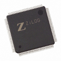
Z8018233ASG Zilog, Z8018233ASG Datasheet - Page 48

Z8018233ASG
Manufacturer Part Number
Z8018233ASG
Description
IC 33MHZ STATIC MIMIC 100-LQFP
Manufacturer
Zilog
Datasheet
1.Z8018233FSG.pdf
(109 pages)
Specifications of Z8018233ASG
Processor Type
Z180
Features
Smart Peripheral Controller
Speed
33MHz
Voltage
5V
Mounting Type
Surface Mount
Package / Case
100-LQFP
Processor Series
Z8018xx
Core
Z80
Data Bus Width
8 bit
Program Memory Type
ROMLess
Interface Type
UART
Maximum Clock Frequency
33 MHz
Number Of Programmable I/os
24
Number Of Timers
2
Operating Supply Voltage
4.5 V to 5.5 V
Maximum Operating Temperature
+ 70 C
Mounting Style
SMD/SMT
Minimum Operating Temperature
0 C
Lead Free Status / RoHS Status
Lead free / RoHS Compliant
Available stocks
Company
Part Number
Manufacturer
Quantity
Price
Zilog
CPU Control Register
Bit 7. Clock Divide Select. Bit 7 of the CCR allows the
programmer to set the internal clock to divide the external
clock by 2 if the bit is 0 and divide-by-one if the bit is 1.
Upon reset, this bit is set to 0 and the part is in
divide-by-two mode. Since the on-board oscillator is not
guaranteed to operate above 20 MHz, an external source
must be used to achieve the maximum 33 MHz operation
of the part, i.e., an external clock at 66 MHz with 50% duty
cycle.
If an external oscillator is used in divide-by-one mode, the
minimum pulse width requirement must be satisfied.
Bits 6 and 3. STANDBY/IDLE Enable. These two bits are
used for enabling/disabling the IDLE and STANDBY mode.
Setting D6, D3 to 0 and 1, respectively, enables the IDLE
mode. In the IDLE mode, the clock oscillator is kept
oscillating but the clock to the rest of the internal circuit,
including the CLKOUT, is stopped. The Z8S180 enters
IDLE mode after fetching the second opcode of a SLEEP
instruction, if the I/O STOP bit is set.
Setting D6, D3 to 1 and 0, respectively, enables the
STANDBY mode. In the STANDBY mode, the clock
oscillator is stopped completely. The Z8S180 enters
STANDBY after fetching the second opcode of a SLEEP
instruction, if the I/O STOP bit is set.
Setting D6, D3 to 1 and 1, respectively, enables the
STANDBY-QUICK RECOVERY mode. In this mode, its
operations are identical to STANDBY except that the clock
3-48
P R E L I M I N A R Y
PS009801-0301
recovery is reduced to 64 clock cycles after the exit
conditions are gathered. Similarly, in STANDBY mode, the
Z8S180 enters STANDBY after fetching the second opcode
of a SLEEP instruction, if the I/O STOP bit is set.
Bit 5. BREXT. This bit controls the ability of the Z8S180 to
honor a bus request during STANDBY mode. If this bit is
set to 1 and the part is in STANDBY mode, a BUSREQ is
honored after the clock stabilization timer is timed out.
Bit 4. LNPHI. This bit controls the drive capability on the
PHI Clock output. If this bit is set to 1, the PHI Clock output
is reduced to 25% of its drive capability.
Bit 2. Reserved
Bit 1. LNCPUCTL. This bit controls the drive capability of
the CPU Control pins. When this bit is set to 1, the output
drive capability of the following pins is reduced to 25% of
the original drive capability:
Bit 0. LNAD/DATA. This bit controls the drive capability of
the Address/Data bus output drivers. If this bit is set to 1,
the output drive capability of the Address and Data bus
output is reduced to 25% of its original drive capability.
- /BUSACK
- /RD
- /WR
- /M1
- E
- /MREQ
- /IORQ
- /RFSH
- /HALT
- /TEND1
Z
ILOG
I
NTELLIGENT
DS971820600
Z80182/Z8L182
P
ERIPHERAL


