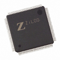
Z8018233ASG Zilog, Z8018233ASG Datasheet - Page 76

Z8018233ASG
Manufacturer Part Number
Z8018233ASG
Description
IC 33MHZ STATIC MIMIC 100-LQFP
Manufacturer
Zilog
Datasheet
1.Z8018233FSG.pdf
(109 pages)
Specifications of Z8018233ASG
Processor Type
Z180
Features
Smart Peripheral Controller
Speed
33MHz
Voltage
5V
Mounting Type
Surface Mount
Package / Case
100-LQFP
Processor Series
Z8018xx
Core
Z80
Data Bus Width
8 bit
Program Memory Type
ROMLess
Interface Type
UART
Maximum Clock Frequency
33 MHz
Number Of Programmable I/os
24
Number Of Timers
2
Operating Supply Voltage
4.5 V to 5.5 V
Maximum Operating Temperature
+ 70 C
Mounting Style
SMD/SMT
Minimum Operating Temperature
0 C
Lead Free Status / RoHS Status
Lead free / RoHS Compliant
Available stocks
Company
Part Number
Manufacturer
Quantity
Price
Zilog
PARALLEL PORTS REGISTERS
The Z80182/Z8L182 has three 8-bit bi-directional Ports.
Each bit is individually programmable for input or output.
The Ports consist of two registers the Port Direction Control
Register and the Port Data Register. The Port and direction
register can be accessed in any page of I/O space since
only the lowest eight address lines are decoded. Bits PC7
and PC6 are input only bits and have the special function
of reading the external value of the /INT2 and /INT1 pins.
Writing ‘1’ to these bits will clear the edge detect interrupt
logic when operating /INT2 and/or /INT1 in edge detect
mode.
When Port B and Port C bits 5-0 are deselected in the
System Configuration Register, the Data and Data Direction
Registers are still available as read/write scratch registers.
If a Port is deselected and if the DDR bit is a ‘0’, then the
written value to that bit will be latched and this value can be
read back. If a Port is deselected and if the DDR bit is a ‘1’,
then you could read only the external pin value; any write
to that bit is latched but can be read back only with DDR=0.
3-76
The data direction register determines which are inputs
and outputs in the PA Data Register. When a bit is set to 1
the corresponding bit in the PA Data Register is an input.
If the bit is 0, then the corresponding bit is an output.
When the Z180 MPU writes to the PA Data Register the
D7 D6 D5 D4 D3 D2 D1 D0
D7 D6 D5 D4 D3 D2 D1 D0
1
X
Figure 83. PA, Port A, Data Direction Register
1
X
(Z180 MPU Read/Write, Address xxEDH)
(Z180 MPU Read/Write, Address xxEEH)
Figure 84. PA, Port A, Data Register
1
X
1
X
1
X
1
X
1
X
1
X
PA Data Direction Register
0=Output
1=Input
PA Data Register
PS009801-0301
P R E L I M I N A R Y
data is stored in the internal buffer. The values of the PA
Data Register are undefined after reset. Any bits that are
output are then sent on to the output buffers.
When the Z180 MPU reads the PA Data Register the data
on the external pins is returned.
The data direction register determines which are inputs
and outputs in the PB Data Register. When a bit is set to 1
the corresponding bit in the PB Data Register is an input.
If the bit is 0 then the corresponding bit is an output.
When the Z180 MPU writes to the PB Data Register the
data is stored in the internal buffer. The values of Port B
data register are undefined after reset. Any bits that are
output are then sent on to the output buffers.
When the Z180 MPU reads the PB Data Register, the data
on the external pins is returned.
Figure 85. PB, Port B, Data Direction Register
Figure 87. PC, Port C, Data Direction Register
D7 D6 D5 D4 D3 D2 D1 D0
1
D7 D6 D5 D4 D3 D2 D1 D0
X
D7 D6 D5 D4 D3 D2 D1 D0
X
(Z180 MPU Read/Write, Address xxDDH)
1
(Z180 MPU Read/Write, Address xxE4H)
Figure 86. PB, Port B, Data Register
X
X
1
X
(Z180 MPU, Address xxE5H)
1
1
X
1
1
X
1
1
X
1
1
X
1
1
X
1
PB Data Direction Register
0=Output
1=Input
Z
ILOG
PB Data Register
PC Direction Register
I
NTELLIGENT
DS971820600
Z80182/Z8L182
P
ERIPHERAL


