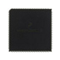
MC68HC711KS2CFN3 Freescale Semiconductor, MC68HC711KS2CFN3 Datasheet - Page 191

MC68HC711KS2CFN3
Manufacturer Part Number
MC68HC711KS2CFN3
Description
Manufacturer
Freescale Semiconductor
Datasheet
1.MC68HC711KS2CFN3.pdf
(290 pages)
Specifications of MC68HC711KS2CFN3
Cpu Family
HC11
Device Core Size
8b
Frequency (max)
4MHz
Interface Type
SCI/SPI
Program Memory Type
ROM
Program Memory Size
32KB
Total Internal Ram Size
1KB
# I/os (max)
51
Number Of Timers - General Purpose
8
Operating Supply Voltage (typ)
5V
Operating Supply Voltage (max)
5.5V
Operating Supply Voltage (min)
4.5V
On-chip Adc
8-chx8-bit
Instruction Set Architecture
CISC
Operating Temp Range
-40C to 85C
Operating Temperature Classification
Industrial
Mounting
Surface Mount
Pin Count
68
Package Type
PLCC
Lead Free Status / Rohs Status
Not Compliant
Available stocks
Company
Part Number
Manufacturer
Quantity
Price
Company:
Part Number:
MC68HC711KS2CFN3
Manufacturer:
NSC
Quantity:
1 001
- Current page: 191 of 290
- Download datasheet (4Mb)
9.4.5 Pulse Accumulator Control Register
9.5 Input Capture (IC)
M68HC11K Family
MOTOROLA
Address: $0026
I4/O5 — Input Capture 4/Output Compare 5 Bit
To configure PA3 as input compare 4, clear DDA3 and set I4/05. To
configure PA3 as output compare 5, set DDA3 and clear I4/05. If the
DDA3 bit is set (configuring PA3 as an output) and IC4 is enabled,
writing a one to TI4/O5 causes an input capture. Writing to TI4/O5 has
no effect when DDA3 is cleared and/or OC5 is enabled.
The input capture function records the time an external event occurs by
latching the value of the free-running counter into one of the timer input
capture (TIC) registers when a selected edge is detected at its
associated timer input pin. Software can store latched values and use
them to compute the period and duration of events. For example, by
storing the times of successive edges of an incoming signal, software
can determine the period and pulse width of a signal. To measure the
period, two successive edges of the same polarity are captured. To
measure pulse width, two alternate polarity edges are captured.
Capture requests are latched on the opposite half cycle of PH2 from
when the timer counter is being incremented. This synchronization
process introduces a delay between edge occurrence and counter value
detection. Because these delays offset each other when the time
between two edges is measured, they can be ignored. There is a similar
delay for output compare between the actual compare point and when
the output pin changes state.
Reset:
Read:
Write:
Freescale Semiconductor, Inc.
Figure 9-7. Pulse Accumulator Control Register (PACTL)
For More Information On This Product,
0 = Configure PA3 as OC5
1 = Configure PA3 as IC4
Bit 7
0
0
Go to: www.freescale.com
PAEN
Timing System
6
0
PAMOD
5
0
PEDGE
4
0
3
0
0
I4/O5
2
0
Input Capture (IC)
RTR1
1
0
Timing System
Technical Data
RTR0
Bit 0
0
191
Related parts for MC68HC711KS2CFN3
Image
Part Number
Description
Manufacturer
Datasheet
Request
R

Part Number:
Description:
APPENDIX A ELECTRICAL CHARACTERISTICS
Manufacturer:
FREESCALE [Freescale Semiconductor, Inc]
Datasheet:
Part Number:
Description:
Manufacturer:
Freescale Semiconductor, Inc
Datasheet:
Part Number:
Description:
Manufacturer:
Freescale Semiconductor, Inc
Datasheet:
Part Number:
Description:
Manufacturer:
Freescale Semiconductor, Inc
Datasheet:
Part Number:
Description:
Manufacturer:
Freescale Semiconductor, Inc
Datasheet:
Part Number:
Description:
Manufacturer:
Freescale Semiconductor, Inc
Datasheet:
Part Number:
Description:
Manufacturer:
Freescale Semiconductor, Inc
Datasheet:
Part Number:
Description:
Manufacturer:
Freescale Semiconductor, Inc
Datasheet:
Part Number:
Description:
Manufacturer:
Freescale Semiconductor, Inc
Datasheet:
Part Number:
Description:
Manufacturer:
Freescale Semiconductor, Inc
Datasheet:
Part Number:
Description:
Manufacturer:
Freescale Semiconductor, Inc
Datasheet:
Part Number:
Description:
Manufacturer:
Freescale Semiconductor, Inc
Datasheet:
Part Number:
Description:
Manufacturer:
Freescale Semiconductor, Inc
Datasheet:
Part Number:
Description:
Manufacturer:
Freescale Semiconductor, Inc
Datasheet:
Part Number:
Description:
Manufacturer:
Freescale Semiconductor, Inc
Datasheet:


