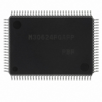
M30624FGAFP#U3 Renesas Electronics America, M30624FGAFP#U3 Datasheet - Page 107

M30624FGAFP#U3
Manufacturer Part Number
M30624FGAFP#U3
Description
IC M16C MCU FLASH 100QFP
Manufacturer
Renesas Electronics America
Series
M16C™ M16C/60r
Datasheets
1.M30622SAFPU5.pdf
(277 pages)
2.M30622SAFPU5.pdf
(617 pages)
3.M30622SAFPU5.pdf
(308 pages)
Specifications of M30624FGAFP#U3
Core Processor
M16C/60
Core Size
16-Bit
Speed
16MHz
Connectivity
SIO, UART/USART
Peripherals
DMA, PWM, WDT
Number Of I /o
85
Program Memory Size
256KB (256K x 8)
Program Memory Type
FLASH
Ram Size
20K x 8
Voltage - Supply (vcc/vdd)
4.2 V ~ 5.5 V
Data Converters
A/D 10x10b, D/A 2x8b
Oscillator Type
Internal
Operating Temperature
-40°C ~ 85°C
Package / Case
100-QFP
For Use With
867-1000 - KIT QUICK START RENESAS 62PM3062PT3-CPE-3 - EMULATOR COMPACT M16C/62P/30P
Lead Free Status / RoHS Status
Lead free / RoHS Compliant
Eeprom Size
-
Available stocks
Company
Part Number
Manufacturer
Quantity
Price
Part Number:
M30624FGAFP#U3M30624FGAFP#D3
Manufacturer:
Renesas Electronics America
Quantity:
10 000
Part Number:
M30624FGAFP#U3M30624FGAFP#D5
Manufacturer:
Renesas Electronics America
Quantity:
10 000
Timers’ functions for three-phase motor control
104
Sawtooth modulation
To generate a PWM waveform of sawtooth wave modulation, set “1” in the modulation mode select bit (bit
6 at 0348
timer registers of timers A4, A1, and A2 comprise conventional timers A4, A1, and A2 alone, and reload
the corresponding timer register’s content to the counter every time the timer B2 counter’s content be-
comes 0000
output polarity select bit (bit 0 at 0348
An example of U phase waveform is shown in Figure 1.15.8, and the description of waveform output
workings is given below. Set “1” in DU0 (bit 0 at 034A
set “0” in DU1 (bit 0 at 034A
When the timber B2 counter’s content becomes 0000
starts outputting one-shot pulses at the same time. In this instance, the contents of the three-phase buffer
registers DU1 and DU0 are set in the three-phase output shift register (U phase), and the contents of
DUB1 and DUB0 are set in the three-phase output shift register (U phase). After this, the three-phase
buffer register’s content is set in the three-phase shift register every time the timer B2 counter’s content
becomes 0000
The value of DU0 and that of DUB0 are output to the U terminal (P8
respectively. When the timer A4 counter counts the value written to timer A4 (038F
timer A4 finishes outputting one-shot pulses, the three-phase output shift register’s content is shifted one
position, and the value of DU1 and that of DUB1 are output to the U phase output signal and to the U
output signal respectively. At this time, one-shot pulses are output from the timer for setting dead time
used for setting the time over which the “L” level of the U phase waveform doesn’t lap over the “L” level of
the U phase waveform, which has the opposite phase of the former. The U phase waveform output that
started from the “H” level keeps its level until the timer for setting dead time finishes outputting one-shot
pulses even though the three-phase output shift register’s content changes from “1” to “0 ”by the effect of
the one-shot pulses. When the timer for setting dead time finishes outputting one-shot pulses, 0 already
shifted in the three-phase shift register goes effective, and the U phase waveform changes to the “L”
level. When the timer B2 counter’s content becomes 0000
registers DU1 and DU0 are set in the three-phase output shift register (U phase), and the contents of
DUB1 and DUB0 are set in the three-phase output shift register (U phase) again.
A U phase waveform is generated by these workings repeatedly. With the exception that the three-phase
output shift register on the U phase side is used, the workings in generating a U phase waveform, which
has the opposite phase of the U phase waveform, are the same as in generating a U phase waveform. In
this way, a waveform can be picked up from the applicable terminal in a manner in which the “L” level of
the U phase waveform doesn’t lap over that of the U phase waveform, which has the opposite phase of
the U phase waveform. The width of the “L” level too can be adjusted by varying the values of timer B2
and timer A4. In dealing with the V and W phases, and V and W phases, the latter are of opposite phase
of the former, have the corresponding timers work similarly to dealing with the U and U phases to gener-
ate an intended waveform.
Setting “1” both in DUB0 and in DUB1 provides a means to output the U phase alone and to fix the U
phase output to “H” as shown in Figure 1.15.9.
___
16
). Also, set “0” in the timers A4-1, A1-1, and A2-1 control bit (bit 1 at 0349
16
. The effective interrupt output specification bit (bit 1 at 0348
16
.
___
16
) and set “1” in DUB1 (bit 1 at 034A
16
) go nullified.
___
16
), and set “0” in DUB0 (bit 1 at 034A
16
___
, timer B2 generates an interrupt, and timer A4
16
___
, the contents of the three-phase buffer
___
16
___
SINGLE-CHIP 16-BIT CMOS MICROCOMPUTER
).
0
) and to the U terminal (P8
16
) and the effective interrupt
___
16
16
, 038E
___
M16C / 62A Group
). In this mode, the
Mitsubishi microcomputers
___
16
16
). In addition,
) and when
1
___
___
)


