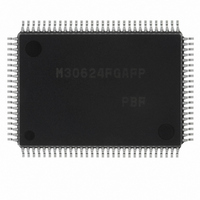
M30624FGAFP#U3 Renesas Electronics America, M30624FGAFP#U3 Datasheet - Page 141

M30624FGAFP#U3
Manufacturer Part Number
M30624FGAFP#U3
Description
IC M16C MCU FLASH 100QFP
Manufacturer
Renesas Electronics America
Series
M16C™ M16C/60r
Datasheets
1.M30622SAFPU5.pdf
(277 pages)
2.M30622SAFPU5.pdf
(617 pages)
3.M30622SAFPU5.pdf
(308 pages)
Specifications of M30624FGAFP#U3
Core Processor
M16C/60
Core Size
16-Bit
Speed
16MHz
Connectivity
SIO, UART/USART
Peripherals
DMA, PWM, WDT
Number Of I /o
85
Program Memory Size
256KB (256K x 8)
Program Memory Type
FLASH
Ram Size
20K x 8
Voltage - Supply (vcc/vdd)
4.2 V ~ 5.5 V
Data Converters
A/D 10x10b, D/A 2x8b
Oscillator Type
Internal
Operating Temperature
-40°C ~ 85°C
Package / Case
100-QFP
For Use With
867-1000 - KIT QUICK START RENESAS 62PM3062PT3-CPE-3 - EMULATOR COMPACT M16C/62P/30P
Lead Free Status / RoHS Status
Lead free / RoHS Compliant
Eeprom Size
-
Available stocks
Company
Part Number
Manufacturer
Quantity
Price
Part Number:
M30624FGAFP#U3M30624FGAFP#D3
Manufacturer:
Renesas Electronics America
Quantity:
10 000
Part Number:
M30624FGAFP#U3M30624FGAFP#D5
Manufacturer:
Renesas Electronics America
Quantity:
10 000
UART2 Special Mode Register
138
Table 1.16.10. Delay circuit select conditions
Digital delay is
selected
Analog delay is
selected
No delay
Figure 1.16.27 shows the functional block diagram for I
(IICM) causes ports P7
output terminal SCL, and port P7
so the SDA output changes after SCL fully goes to “L”. The SDA digital delay select bit (bit 7 at address
0377
amount of delay can be selected in the range of 2 cycles to 8 cycles of f1 using UART2 special mode
register 3 (at address 0375
An attempt to read Port P7
port direction register. The initial value of SDA transmission output in this mode goes to the value set in
port P7
of UART2 reception interrupt turn to the start/stop condition detection interrupt, acknowledgment non-
detection interrupt, and acknowledgment detection interrupt respectively.
The start condition detection interrupt refers to the interrupt that occurs when the falling edge of the SDA
terminal (P7
refers to the interrupt that occurs when the rising edge of the SDA terminal (P7
terminal (P7
start condition detection, and set to “0” by the stop condition detection.
The acknowledgment non-detection interrupt refers to the interrupt that occurs when the SDA terminal
level is detected still staying “H” at the rising edge of the 9th transmission clock. The acknowledgment
detection interrupt refers to the interrupt that occurs when SDA terminal’s level is detected already went
to “L” at the 9th transmission clock. Also, assigning 1 1 0 1 (UART2 reception) to the DMA1 request factor
select bits provides the means to start up the DMA transfer by the effect of acknowledgment detection.
Bit 1 of the UART2 special mode register (0377
Arbitration means the act of detecting the nonconformity between transmission data and SDA terminal
data at the timing of the SCL rising edge. This detecting flag is located at bit 11 of the UART2 reception
buffer register (037F
arbitration lost detecting flag control bit to choose which way to use to update the flag, bit by bit or byte by
byte. When setting this bit to “1” and updated the flag byte by byte if nonconformity is detected, the
arbitration lost detecting flag is set to “1” at the falling edge of the 9th transmission clock.
If update the flag byte by byte, must judge and clear (“0”) the arbitration lost detecting flag after complet-
ing the first byte acknowledge detect and before starting the next one byte transmission.
Bit 3 of the UART2 special mode register is used as SCL- and L-synchronous output enable bit. Setting
this bit to “1” goes the P7
16
) can be used to select between analog delay and digital delay. When digital delay is selected, the
0
. The interrupt factors of the bus collision detection interrupt, UART2 transmission interrupt, and
1
0
) staying “H”. The bus busy flag (bit 2 of the UART2 special mode register) is set to “1” by the
) is detected with the SCL terminal (P7
IICM
1
1
0
Register value
16
0
, 037E
, P7
1
SDDS
data register to “0” in synchronization with the SCL terminal level going to “L”.
1
16
1
1
0
0
1
(SCL) results in getting the terminal’s level regardless of the content of the
, and P7
). Delay circuit select conditions are shown in Table 1.16.10.
16
), and “1” is set in this flag when nonconformity is detected. Use the
2
000
(000)
(000)
001
111
DL
respectively. A delay circuit is added to the SDA transmission output,
to
2
to work as data transmission-reception terminal SDA, clock input-
When IICM = “0”, no delay circuit is selected. When IICM = “0”,
however, always make sure SDDS = “0”.
When digital delay is selected, no analog delay is added. Only
digital delay is effective.
When DL is set to “000”, analog delay is selected no matter what
value is set in SDDS.
When SDDS is set to “0”, DL is initialized, so that DL =“000”.
16
) is used as the arbitration lost detecting flag control bit.
1
) staying “H”. The stop condition detection interrupt
2
C mode. Setting “1” in the I
Contents
SINGLE-CHIP 16-BIT CMOS MICROCOMPUTER
0
) is detected with the SCL
M16C / 62A Group
2
Mitsubishi microcomputers
C mode select bit


